北极星架构白皮书(Polaris Architecture whitepaper):http://radeon.com/polaris-architecture-whitepaper/
pdf版:http://radeon.wpengine.netdna-cd … -Final-08042016.pdf
自翻,转载请注明出处

首先发这篇帖子只是想对某些可能有误导趋势的帖子进行一个纠正,并将北极星架构白皮书书中某些比较重要的内容选出来翻译一下。
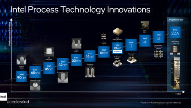
在白皮书中,首先谈到的就是14nmFinFET制程带来的各种提升,还谈到了为什么选择14nm而不是台积电16nm。

RX480 GPU,Polaris 10

晶片照片
Underlying Polaris architecture is the choice of process technology, which determines what is physically possible. Active (or dynamic) power consumption increases linearly with the number of computational units, but cubically when boosting frequency through higher voltage (e.g., 15% higher frequency and voltage increases power consumption by 52%). As a result, graphics processors tend to prefer lower frequencies and use greater density to deploy more computational units that operate in parallel. For the last five years, graphics processors have relied on 28nm high-k/metal nodes (see fig. 2).
【北极星架构的基础是制程,制程决定了物理上的可能性。随着计算单元的增加,平均功率线性增长,而通过加压来提高频率时,功耗则会以三次方形式增长(比如提高15%频率、电压,功耗则将上升52%).因此,GPU一般频率比较低,并采用高密度的制程,来放入更多并行计算单元。过去的五年里,GPU用的全都是28nm HKMG工艺。】

【Radeon显卡自从2005年以来的进化】
For Polaris GPUs, AMD selected and Global Foundries’ 14nm FinFET-based process technology, which is the densest foundry GPU process available for production to date. FinFET transistors are crucial to reducing power consumption and enable operating voltages that are 150mV lower than the previous generation, thereby cutting active power by approximately 30% from a 1V baseline.
【在Polaris GPU上,AMD选择了GF的14nm FinFET制程,这是目前密度最高的GPU制程,FinFET对于降低功耗十分重要,相对前代,14nm FinFET的工作电压降低了150mV,因此也将平均功率下降了大概30%。】

【FinFET制程 关键参数】
Table 1 contains publicly available details on key dimensions for modern FinFET process nodes. For example, the table illustrates that the 14nm transistor spacing (i.e. contacted gate pitch) is approximately 15% smaller than TSMC 16nm spacing, while the SRAM used for caches and register files is 10% smaller. Overall, these process technology advantages translate into GPUs with more compute units, which allows for parallelism and better power efficiency.
【上表包含了公开的当代FinFET制程细节。表中说明GF14nm比台漏电16nm的晶体管间距(比如栅极触点节距)要小15%,用作缓存和寄存器的SRAM则要小10%。总而言之,以上的优势转换到GPU中就是更多的计算单元,拥有更强大的并性能力,更好的能效。】
谈完工艺,让我们看看之前谣传“完整2560SP”的P10核心问题。

【RX480的CU预留,应用程序预留了4组CU,用来实时音频光线追踪】
【注:这个应该是用于VR的,类似于NV的 VRWorks Audio音频技术,借鉴了光线追踪渲染的思路,充分考虑了3D场景的渲染,通过将音频交互映射到3D场景中的物体上,实现了完全符合听觉和声学原理的音频,听起来更加自然,包括方向、远近等等。】
The second quality-of-service technique, compute unit reservation, is even more potent and general-purpose. As the name suggests, programmers can partition the execution resources of the Polaris GPU for compute tasks using API extensions. Specifically, compute units (CUs) in the shader array are reserved for a queue in one of the ACEs, ensuring dedicated resources are available for work-groups from the queue. This is a powerful tool for developers to avoid contention between multiple tasks.
【CU预留是非常有潜力并且多用途的特性。正如其名,程序猿们可以使用API拓展,将Polaris的执行单元进行分区。说得更明白点,CU单元可以为乱序执行引擎ACE中的一个队列而保留,确保队列中的任务能够使用专用的资源。对于开发者来说,这是避免多任务中资源争夺的一个有力工具。】
Figure 4 illustrates an example, where a queue for audio tasks is assigned 4 CUs, while the remaining compute units are available to all tasks. Partitioning the CUs ensures that audio tasks will have the lowest possible latency and jitter, although the CUs are no longer available for other tasks
【上图只是一个例子,在这种情况下,音频任务队列会分派到4个CU中,剩余的CU则能执行所有任务。预留CU能确保音频任务会有最低的延迟和抖动,但这些CU无法执行其他任务。】
首先,这个表中的P10 GPU一共只有36个CU,2304SP(数学!数学!),上文的意思是,可能在运行VR时,会使用4组CU,256SP来处理VR音频,剩余的32组,2048SP处理其他任务,而不是说完整的有40组。
说完规格,再看看架构

In a similar vein, the Polaris geometry engines can detect triangles that have no area, and discard them during the input assembly stage. As vertex indices are read from the input buffer, the Polaris geometry engine will check if two or more vertices have the same coordinates (i.e., degenerate triangles). The degenerate triangles are culled before they are passed to the vertex shaders, which increases throughput by reducing the amount of work done and reducing the energy consumed. By eliminating the vertex fetches for degenerate triangles, Polaris can increase throughput by up to 3X for certain scenes.
【这里是前端加强,之前帖子就提到过,Polaris增加了Primative Discard Accelerator,在渲染管线前,甚至是到达顶点渲染器之前,就能够去除无用(无法渲染/不可见)的部分多边形,声称MSAA开的越高,带来的提升就越高,因为正是MSAA加重了这种无用多边形给GPU带来的负担,在特定场景下可以提高最多3倍的吞吐量。】
除了前端,还有Delta色彩压缩带来的等效带宽的提升。

【AMD Delta色彩压缩的进步,在Polaris上等效带宽提升了最多35%】
The Polaris memory interface has been updated to both increase bandwidth and also operate more efficiently with compression (fig. 7). The Polaris render back-end is designed to compress color buffers to save power and more effectively use the available memory bandwidth. Delta color compression is a lossless algorithm that dynamically divides a color buffer into several blocks and was first deployed in 3rd-generation GCN solutions (e.g. GPUs codenamed “Tonga,” “Fiji,” and “Antigua”). A single pixel in each block is written using a normal representation and all other pixels in the block are encoded as a difference from the first value. The block size is dynamically chosen based on access patterns and the data patterns to maximize the benefits. The peak compression ratio is 8:1 for a 256-byte block. Since many objects have large patches of similar colors (e.g. clothing and cars), the delta color compression takes advantage of this locality to improve performance. While 3rd-generation GCN and Polaris use similar algorithms, Polaris is more aggressive and compresses even more blocks, thereby saving more bandwidth and power.
【Polaris的内存控制器不仅提升了带宽,而且在色彩压缩的帮助下更有效率。渲染后端RBE能够压缩色彩缓存,更节能高效地利用带宽。Delta色彩压缩是一种无损压缩方式,在第三代GCN上首次引入(比如“Tonga”“Fiji”“Antigua”核心)。每个块的一个像素点以正常值写入,而该块的其他像素点则用以该像素点为参照的不同值解码。块的大小依据访问和数据模式动态选择,来最大化效率。一个256字节的块,峰值压缩比为8:1。由于很多物体都有很多相同颜色的色块(比如衣服、汽车),Delta色彩压缩将会很有优势。第三代GCN和Polaris采用了不同的算法,Polaris的算法更加激进,能压缩更多块,节省更多带宽和功耗。】
The biggest savings come when the color buffer is read back for subsequent computations, i.e. render to texture mode. The Polaris shader cores can read and transparently decompress the compressed color data thereby saving read bandwidth in the memory and caches as well.
【当色彩缓存由于之后的计算而被读回时,这时带宽节省最明显,比如渲染到纹理模式。Polaris的SP可以读取并快速解压色彩数据,节省内存和缓存带宽。】

In fact, the compression is so efficient that the Polaris architects were able to reduce the number of render back-ends. Polaris has a compact 256-bit memory interface that uses cost-effective GDDR5 memory, but delivers similar end-user performance to the GPU codenamed “Hawaii”, which used a 512-bit memory interface ? all while consuming less power (fig. 8).
【实际上,由于色彩压缩带来的能效提升,Polaris架构上甚至减少了渲染后端单元的数量。Polaris的内存位宽只有256bit,但实际性能和512bit的Hawaii差不多,节省了最多58%的功耗。】
全文完,转载请注明出处,另外请国内某些网站的小便最好有点节操。