【NVIDIA正准备Volta产品线 – GV104,GV102和GV110,架构大改】NVIDIA Prepping High-Performance Volta GPU Lineup ? GV104, GV102 and GV110 To Feature Completely Revamped SM Architecture
source:http://wccftech.com/nvidia-volta-gv110-gv104-gv102-gpu/
自翻,转载请注明出处。
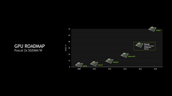
NVIDIA has yet to launch their entire Pascal graphics card lineup and rumors have already started hinting at their upcoming GPU architecture. Announced more than years ago, the Volta GPU was to be NVIDIA’s next greatest chip architecture to replace Maxwell but was pushed back with Pascal taking its place. With Pascal development complete, NVIDIA has set their efforts in the developing their latest GPU project.
【虽然NVIDIA最近才把Pascal产品线补全,但已经开始有关于下代Volta GPU的传闻了。作为Maxwell的换代架构,Volta架构在几年前就被提出了,但后来又从中插入了一个Pascal,取代了它的位置。目前Pascal的所有开发工作已经完成,NVIDIA正转向开发下代Volta GPU。】
【Volta架构会有三款高性能GPU – GV102,GV104,GV110】
The rumor on NVIDIA Volta GPU comes straight from the Motley Fool who were able to obtain some big details on the next-gen chip architecture through a Chinese source. According to the rumor, NVIDIA is prepping a range of chips that will utilize the Volta architecture. Not only that, the Volta GPU architecture has been significantly revamped and will offer a serious improvement in terms of performance and power efficiency compared to the Pascal GPUs.
【传闻来自于Motley Fool,他们能从天朝的消息来源获取下代架构的某些细节。按照传闻,NVIDIA正在准备一系列Volta架构的GPU。不仅如此,Volta架构相对于Pascal架构,将会有重大改变,带来性能和能效的大幅提升。】
The site mentions development of three GPUs based on the Volta architecture is underway. Last night, NVIDIA confirmed during their earnings call that they have taped out and finished development for all Pascal GPUs but they will be introducing all of them at various time frames. This statement confirms that NVIDIA’s development department is now focused on finishing Volta in time. However, I would like to point out that development on these GPUs had begun much earlier as it took NVIDIA three years to to develop the Pascal architecture with a total cost between 2-3 billion dollars.
【网站提到说Volta架构有3颗GPU正在开发之中。昨晚,NVIDIA在电话会议上证实,所有Pascal GPU都已经开发完毕并送交制造,会在不同时间发布。这也证明NVIDIA已经转向Volta的开发。然而我想指出的是,这三个GPU的开发肯定是很早之前就开始了的,因为NVIDIA开发Pascal就用了三年,总计花费20-30亿美元。】
Volta GPUs would feature a huge leap in performance per watt compared to current gen chips.
【Volta将会在能耗上实现大的飞跃】
Following are the chips that are rumored to be introduce as high-end gaming GPUs:
【下面是Volta的高端游戏GPU】
NVIDIA GV110 GPU
NVIDIA GV102 GPU
NVIDIA GV104 GPU
Volta has long been part of NVIDIA’s roadmap and there’s no doubt that most of the work on these chips will be nearing competition as we enter 2017. During these phase, engineering secrets leak out and we are looking at a similar situation where someone was hinted about Volta’s architecture enhancements. According to the rumor, Volta is significantly redesigned compared to the Pascal architecture.
【Volta在NVIDIA的路线图上存在了很久了,毫无疑问,进入2017年后,这些GPU就接近完成了。在这段时间,会有秘密曝光,今天带来的就是这样的一则消息。按照传闻,Volta将会是大改版【与Maxwell改良版Pascal相比而言】】
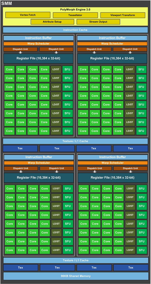
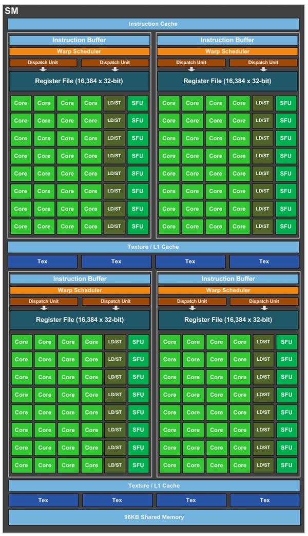
NVIDIA’s Pascal architecture has significant gains in almost all departments over Maxwell but it’s also fact that Pascal and Maxwell share a common DNA. The SM design for both chips is very same. Aside from the GP100 GPU which is different due to its FP64 hardware blocks, the GP106, GP104 and GP102 share a lot in common with Maxwell designs.
【Pascal在每个方面都比Maxwell有显著加强,但这也说明了Pascal和Maxwell在骨子里还是相同的。SM设计都很相似。撇开GP100的FP64单元导致的不同,GP106,GP104,GP102和Maxwell的设计都有很多共同之处。】
Maxwell SMM
Pascal SM
The streaming multiprocessor block for Pascal and Maxwell was similar but was vastly tuned along with the upgrade to the new FinFET node which led to some good increases. Volta on the other hand will feature a completely new design across the board.
【Pascal和Maxwell的SM组设计相似,但由于换了16nm FinFET,各方面的性能都有上升,但Volta将会是完完全全不同的设计。】
NVIDIA GV102, GV104 For High-End Gamers, GV110 Also Aimed at Consumer Market?
【高玩的GV102,GV104,消费级市场也有GV110?】
Starting with the GV104 GPU, we know from the name that this chip will replace the GP104 GPU and will be the most ideal chip for gamers with a decent price tag. NVIDIA’s most successful cards came from the G*104 series of GPUs since the Fermi series. Moving on, we can see vastly improved performance from such chips. The next chip in the stack is GV102. Succeeding the GP102 which is housed inside the GeForce GTX Titan X (P) card, the new high-performance chip will be aimed at enthusiasts who demand serious horsepower.
【从GV104说起,从名字就看得出它将取代GP104,对于预算充足的游戏玩家会是最理想的选择。从Fermi时代开始,NV最成功的显卡基本都是G*104系列的。GP102Titan X的继任者GV102也将是需要大量计算能力的发烧友的菜。】
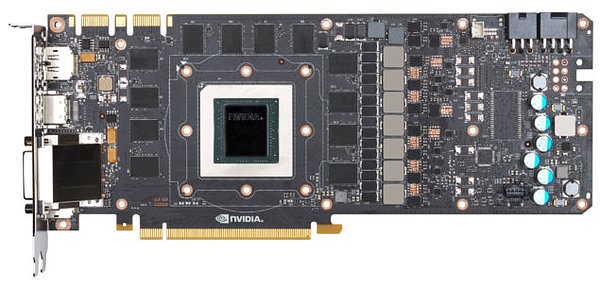
The Titan X features the high-end GP102 chip with insane amounts of horse power.
【采用GP102的Titan X,计算能力丧病】
The third chip is the most interesting as it is also mentioned as a gaming chip. Known as GV110, the GPU will be the ultimate design featuring the Volta architecture. Currently, the GP100 GPU is the top dog of Pascal line and is housed inside the HPC accelerators such as Tesla P100. This chip is built for double precision workloads and designed around NVLINK interconnect.
【GV110则比较有趣,因为它也是游戏显卡。它将是Volta架构的最强者。目前GP100是Pascal的最强GPU,用在HPC加速方面,Tesla P100主要用于双精度负载,采用NVLINK互联。】
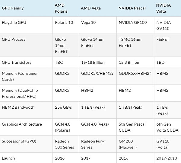
The GP100 GPU is also the only chip that utilizes the fastest HBM2 memory. Now GV110 is interesting as it recalls the naming scheme of GK110. GK110 was also a chip which featured the double precision capabilities, however they were cut down on the consumer variants.
【GP100也是唯一一个采用HBM2显存的GPU。目前GV110有点像当年的GK110,K6000上的GK110有着完整的双精度能力,然而到了GTX系列上就被砍了。】
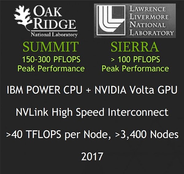
NVIDIA Volta will be featured inside two (100+ PFLOPs) supercomputers.
【Volta将会在两个100+PFLOPs的超算上采用】
With GP102 and GP100, NVIDIA has tried to maintain parity in terms of performance while getting rid of the non-essential features that are not required in gaming and professional workloads (FP64/NVLINK). GV110 can be the full fat chip with limited FP64 capabilities designed for the prosumer market.
【在GP102和GP100上,NV打算在阉割游戏和专业负载(FP64/NVLINK)上用处不大的功能的同时,保持性能不变。GV110将会是完整大核心,但会对FP64性能做限制以投入消费市场。】
It will be interesting to see how this works out but we shouldn’t expect Volta GPUs this soon. The closest we will hear anything official from NVIDIA on Volta would be their GTC presentation in 2017 but aside from that, much of the talks will be focused towards new Pascal GPU launches as they have yet to introduce the full fat variants of GP102 and GP100 in the market.
【关于黄公公将会在Volta上如何施展华丽的刀法,这会是非常有趣的一件事。Volta离我们最近的官方介绍会是2017年的GTC大会,但在那之前,我们还将继续讨论新的Pascal GPU,因为直到现在完整的GP102和GP100都还没发布。】
