【Core2 & Conroe十周年:摩尔定律已死,摩尔定律万岁!】Ten Year Anniversary of Core 2 Duo and Conroe: Moore’s Law is Dead, Long Live Moore’s Law
source:http://www.anandtech.com/show/10525/ten-year-anniversary-of-core-2-duo-and-conroe-moores-law-is-dead-long-live-moores-law
先挖好坑,至于填不填,当然会【更新9.12号 来自EVOLIFE的译文,这坑不用我填了(其实我TM忘了)】
个人感觉一边听着Viva la vida,一边看这个帖子是最好的。

Today marks a full 10 years since the first Core 2 Duo processors, and hence Intel’s 64-bit Core microarchitecture, were made officially available at retail. These included a number of popular dual-core processor parts, including the seemingly ubiquitous E6400 and the Core 2 Extreme X6800. These were built on Intel’s 65nm process, and marked a turning point in the desktop processor ecosystem. To quote Anand inour launch review: ‘you’re looking at the most impressive piece of silicon the world has ever seen’.【10年前,65nm的Conroe成为了桌面处理器生态系统的转折点。从普及型的E6400到旗舰级的Core2 Extreme X6800,这一系列由Intel 65nm工艺打造的处理器中有太多的经典产品。Anandtech当年评价:“这是半导体有史以来最振奋人心的产品”。】
Ten Year Anniversary of Core 2 Duo and Conroe【Core2 & Conroe十周年】
As part of this piece we will also look at some of the predictions for the future, from the latest (and possibly last) International Technology Roadmap for Semiconductors report, which predicts the stalling of smaller silicon manufacturing nodes over the next 10-15 years.
The first part of this article borrows heavily from Johan’s original look into the Intel Core microarchitecture back in 2006. It’s an awesome read.
Back When I Were A Lad
For a number of our readers, the launch of Conroe was a vast change in the processing landscape. The family of Netburst, Northwood and Prescott processors, in the form of Pentium D and Pentium 4, showed that pursuing the frequency race pushed the silicon far outside its efficiency zone and left a hot, power hungry mess in its wake. It didn’t even come with a muscular V8 sound, and AMD’s Athlon 64 X2 line had taken both the performance and efficiency crown.【酷睿2的发布大幅改变了处理器的版图,过去Netburst家族以Northwood和Prescott核心为首的Pentium4和Pentium D处理器一味飙主频的路线已经走火入魔,半导体的发展方向一再偏离效率,带来了巨大的发热和功耗问题,在90nm遇到严重瓶颈后(进入90nm工艺后,业界发现之前摩尔定律一贯的工艺提升,功耗下降的规律失灵了,prescott处理器因为发热过大无法按既定路线突破4Ghz,甚至引发了散热器大规模换代)。Conroe之前,Netburst家族将能效和性能王冠让给了AMD K8】

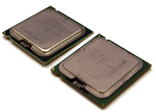
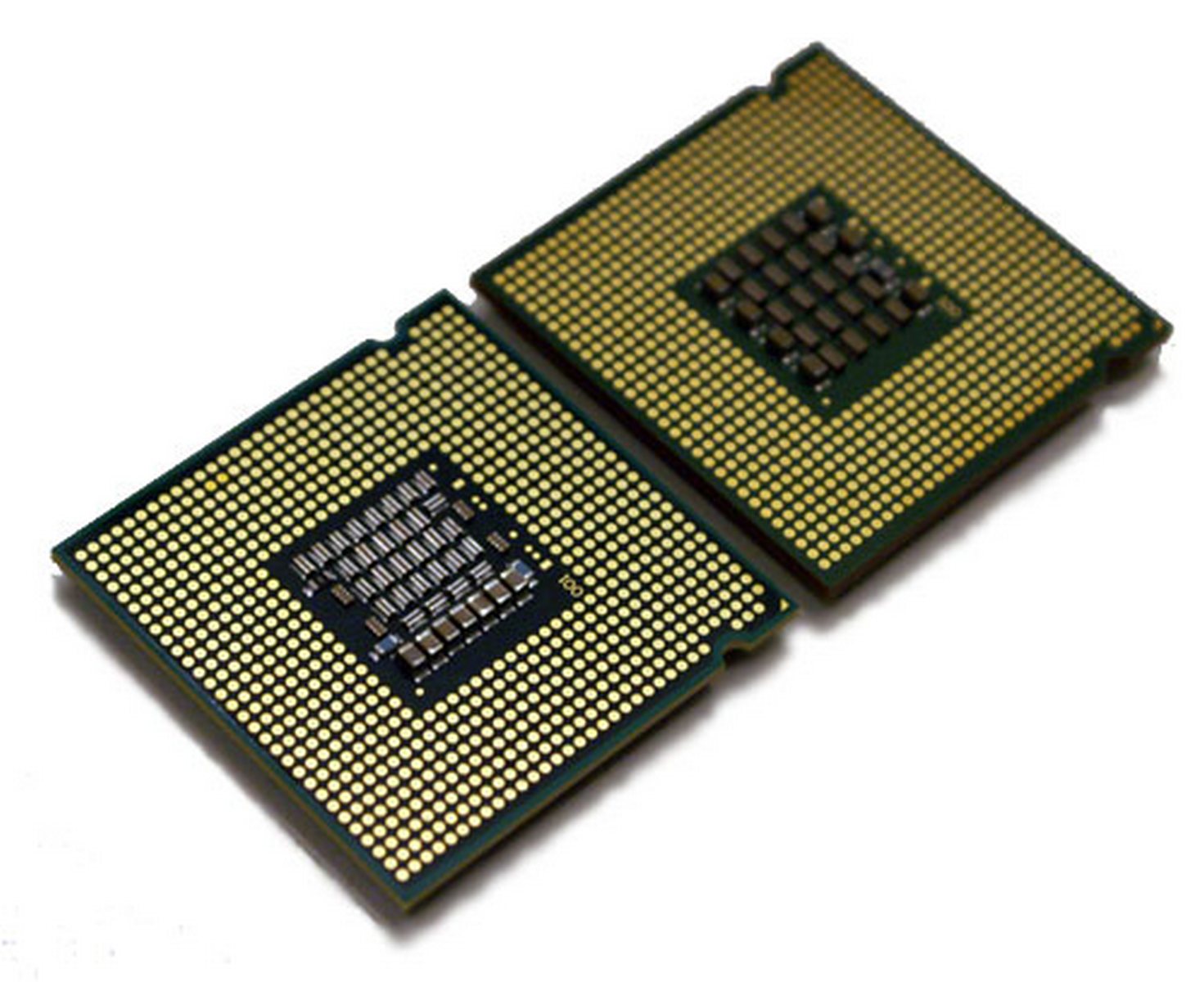
Core 2 Duo (left) vs Pentium D (right)
From the perspective of Intel, it had to incorporate a significant paradigm shift in the way it approached the core microarchitecture ? no more long pipelines to bump up clock rates to start. The Core microarchitecture design was marketed as a blend of Pentium Pro techniques and Netburst architecture, however as Anand pointed out at the time, it is significantly Pentium Pro and it is very hard to find anything Netburst in there. It wasn’t as simple as ‘adding a few functional units or decoders on Yonah and calling it a day’, almost 80% of the architecture and circuit design had to be redone.【Core架构在宣传时被称为Pentium Pro和Netburst技术的结合体,然而很大程度上他就是个Pentium Pro,在里面很难找到Netburst的痕迹。Conroe并不是在Yonah基础上简单的增加了几个功能单元或解码器那么简单(在十年前盛传酷睿2仅仅是Yonah的增强版),几乎有80%的架构和电路设计都重做了。】
As part of this piece, we’re going to take another look at the original architecture improvements of the Core microarchitecture design and some of our old performance metrics from a decade ago.
27th July 2006: Core 2 Launch Day
Ten years ago, Intel launched the following five processors:
【十年前发布的Conroe有如下五款产品:】

The X6800 sits at the top with a higher clock speed with a higher supported FSB-to-core ration than previous Intel processors. The Core 2 processors all came from a 143mm2 die, compared the 162mm2 of Pentium D, and they both seem tiny by comparison to the large die sizes we see 2016 for things like the P100. These were chips without integrated graphics either.
【旗舰产品X6800主频高达2.93Ghz,支持更高的前端总线频率,芯片面积143平方毫米,比前代Pentium D的162平方毫米更小,由于不集成GPU,十年前的处理器比今天的产品小得多。】
The introduction of Core 2 pushed the prices of the Pentium D processors down, to give this interesting table:

Comparing this to recent Intel processors, and the X8600 matches the list price of the Core i7-5960X (an 8-core part), whereas the popular Core 2 Duo E6400 at $224 at the same price as the Core i5-6600.
【当年X6800的价格为999美元,跟今天8核的Core i7-5960X相当,而E6400则为224美元,和Core i5-6600一致,有意思的是,不知道是不是为了快点跟昨天说再见,intel把昨天还是次旗舰产品的3.4Ghz的Pentium D 945砍到比E6300还低的163美元,这是intel桌面处理器历史上独一无二的事件。】
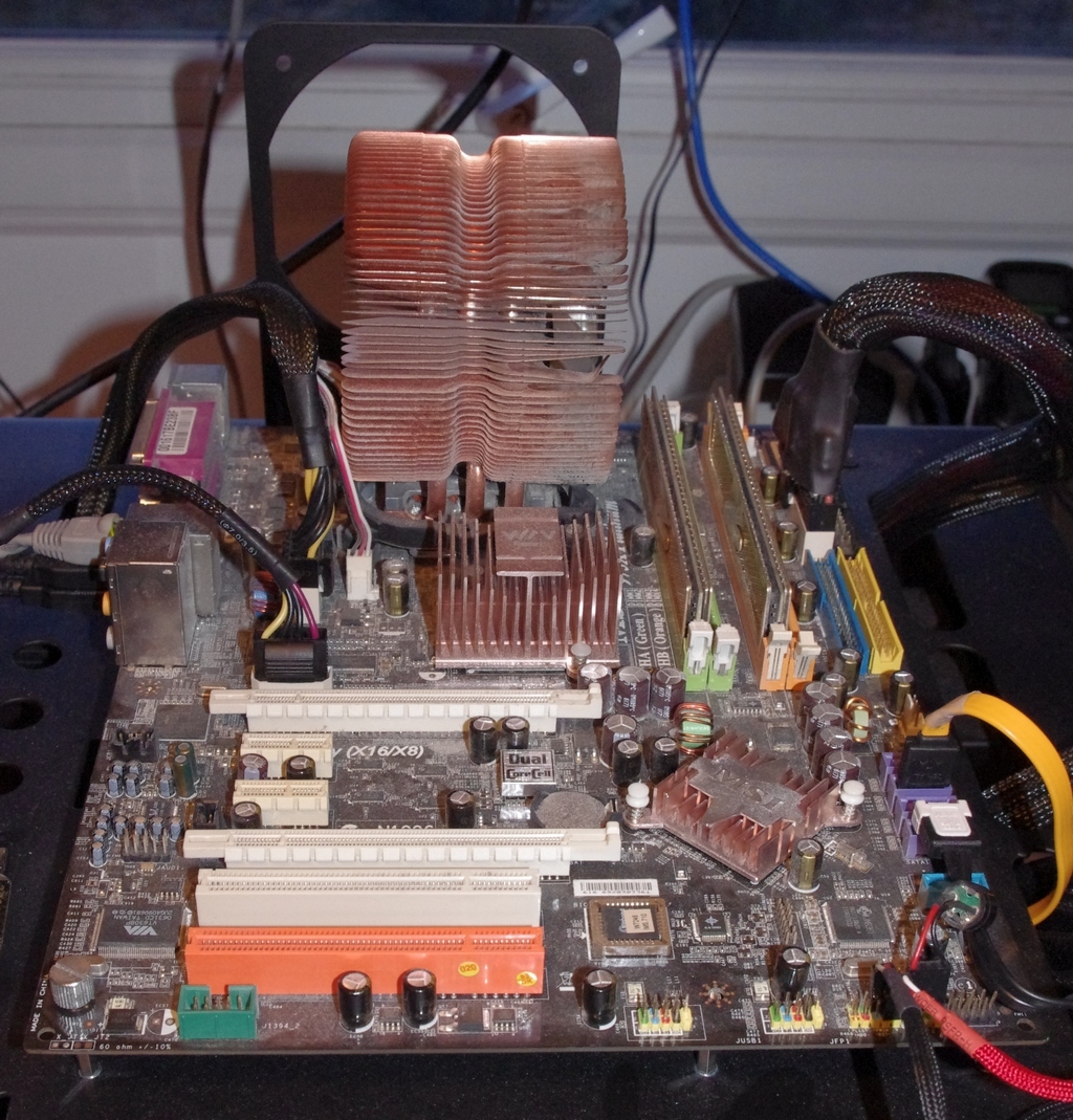
A few years ago, I salvaged a super old computer of mine with an E6400 and took it for a spin for a pipeline piece entitled ‘Dragging Core 2 Duo into 2013’. We know that a number of users today are still using the old platform as their day to day machine, and given that it is now celebrating its 10th birthday, it is interesting that anyone wanting to play around with the old hardware can get a motherboard, memory and CPU from eBay for $50-70.

My crusty C2D Setup from 2013
Core: It’s all in the Prefetch【Core架构:一切皆在预取】
In a simple CPU design, instructions are decoded in the core and data is fetched from the caches. In a perfect world, such as the Mill architecture, the data and instructions are ready to go in the lowest level cache at all times. This allows for the lowest latency and removes a potential bottleneck. Real life is not that rosy, and it all comes down to how the core can predict what data it needs and has enough time to drag it down to the lowest level of cache it can before it is needed. Ideally it needs to predict the correct data, and not interfere with memory sensitive programs. This is Prefetch.
【CPU执行的指令来自解码器,数据取自高速缓存(Cache),在理想环境中,数据和指令都可以从底层缓存中获取(一级缓存,L1 Cache),延迟极低,不存在瓶颈。现实环境可没那么乐观,延迟完全靠猜,核心预测所需数据并且在用到它们之前放入底层缓存的能力决定了现实环境的延迟,这项技术就是预取。】
The Core microarchitecture added multiple prefetchers in the design, as well as improving the prefetch algorithms, to something not seen before on a consumer core. For each core there are two data and one instruction prefetchers, plus another couple for the L2 cache. That’s a total of eight for a dual core CPU, with instructions not to interfere with ‘on-demand’ bandwidth from running software.
【酷睿2微架构增加了多重预取,这是过去在消费级处理器中从没出现过的,并且改进了预取算法,每个核心有两个数据和一个指令预取,加上二级缓存的两个预取,在双核酷睿2中总共有8个预取来维持处理器高效执行。】
One other element to the prefetch is tag lookup for cache indexing. Data prefetchers do this, as well as running software, so in order to avoid a higher latency for the running program, the data prefetch uses the store port to do this. As a general rule (at least at the time), loads happen twice as often as stores, meaning that the store port is generally more ‘free’ to be used for tag lookup by the prefetchers. Stores aren’t critical for most performance metrics, unless the system can’t process stores quickly enough that it backs up the pipeline, but in most cases the rest of the core will be doing things regardless. The cache/memory sub-system is in control for committing the store through the caches, so as long as this happens eventually the process works out.
【另一方面,预取还是为缓存索引做查找标签,数据预取这么做是为了避免程序运行的时候出现高延迟,数据预取是通过存储端口(store port)进行缓存索引,因为原则上载入操作(Load)的频度是存储操作(Store)的两倍,intel在酷睿2中巧妙的把存储端口这一相对空闲给利用起来。】
Core: More Cache Please【Core架构:缓存,多多益善】
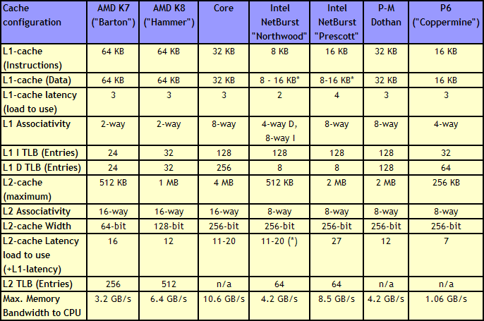
Without having access to a low latency data and instruction store, having a fast core is almost worthless. The most expensive SRAMs sit closest to the execution ports, but are also the smallest due to physical design limitations. As a result, we get a nested cache system where the data you need should be in the lowest level possible, and accesses to higher levels of cache are slightly further away. Any time spent waiting for data to complete a CPU instruction is time lost without an appropriate way of dealing with this, so large fast caches are ideal. The Core design, over the previous Netburst family but also over AMD’s K8 ‘Hammer’ microarchitecture, tried to swat a fly with a Buick.【离开了低延迟数据和指令存取,快速核心将会一文不值,所以最贵的SRAM作为一级缓存被用在离执行单元最近的位置,这里寸土寸金,限制了一级缓存的容量,所以CPU中的高速缓存都被设计成嵌套的结构,容量大得多的二级缓存(L2 Cache)被放在外围,一级缓存不命中(Cache Miss)就得到二级缓存甚至内存中查找数据,这些操作会带来延迟,影响执行速度,在所以缓存大小很重要。Netburst和K8的小缓存上要做到命中就像开着别克拍苍蝇一样,酷睿2拥有比前代产品以及竞争对手都要多的缓存。】

Core gave a 4 MB Level 2 cache between two cores, with a 12-14 cycle access time. This allows each core to use more than 2MB of L2 if needed, something Presler did not allow. Each core also has a 3-cycle 32KB instruction + 32KB data cache, compared to the super small Netburst, and also supports 256 entries in the L1 data TLB, compared to 8. Both the L1 and L2 are accessible by a 256-bit interface, giving good bandwidth to the core.
【Conroe上双核心共享4ML2 每个核心可以使用2M以上的L2,这在胶水双核Presler上是不可能的。L1指令和数据缓存也比Netburst大得多。】
Note that AMD’s K8 still has a few advantages over Core. The 2-way 64KB L1 caches on AMD’s K8 have a slightly better hit rate to the 8-way 32KB L1 caches on Core, with a similar latency. AMD’s K8 also used an on-die memory controller, lowering memory latency significantly, despite the faster FSB of Intel Core (relative to Netburst) giving a lower latency to Core. As stated in our microarchitecture overview at the time, Athlon 64 X2s memory advantage had gotten smaller, but a key element to the story is that these advantages were negated by other memory sub-system metrics, such as prefetching. Measured by ScienceMark, the Core microarchitecture’s L1 cache delivers 2x bandwidth, and the L2 cache is about 2.5x faster, than the Athlon one.
【酷睿2的缓存设计较前代Pentium4的变化体现在一级缓存大幅增加到32KB,,延迟降低到3个时钟周期,二级缓存则为双核共享的4MB,延迟降低到12~14时钟周期。对手AMD的K8虽然有更大容量的一级缓存,内置内存控制器的设计相比Pentium4有较大优势,但带宽偏小,二级缓存容量也有明显差距,实测表明,酷睿2一级缓存带宽为K8的2倍,二级缓存则达到2.5倍。K8与Core2架构相比,还是有部分优势的 – L1缓存、IMC。】
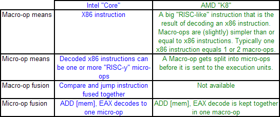
Core: Decoding, and Two Goes Into One【Core架构:解码、融合】
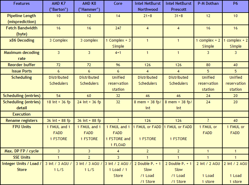
The role of the decoder is to decipher the incoming instruction (opcode, addresses), and translate the 1-15 byte variable length instruction into a fixed-length RISC-like instruction that is easier to schedule and execute: a micro-op. The Core microarchitecture has four decoders ? three simple and one complex. The simple decoder can translate instructions into single micro-ops, while the complex decoder can convert one instruction into four micro-ops (and long instructions are handled by a microcode sequencer). It’s worth noting that simple decoders are lower power and have a smaller die area to consider compared to complex decoders. This style of pre-fetch and decode occurs in all modern x86 designs, and by comparison AMD’s K8 design has three complex decoders.
【解码器的作用是对指令进行解码,并且将这些长度为1~15字节不等的指令翻译成类RISC的定长指令便于执行,在酷睿2中,称之为微操作(micro-op)。预取配合译码是当代X86处理器设计的核心,酷睿2中有四组译码器,其中三组为简单译码器,一组是复杂译码器,前者能将指令翻译成一条微操作,功耗更低晶体管更少,而后者则可以转换出四条(长指令的利器)。这就是俗称的四发射,酷睿2是X86桌面处理器中引领了四发射的潮流。】
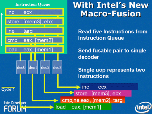
The Core design came with two techniques to assist this part of the core. The first is macro-op fusion. When two common x86 instructions (or macro-ops) can be decoded together, they can be combined to increase throughput, and allows one micro-op to hold two instructions. The grand scheme of this is that four decoders can decode five instructions in one cycle.
【此外,酷睿2加入了宏操作融合(Macro-op Fusion),这样两条常规X86指令(或者宏操作)会被同时译码以增加并发,同时允许一条微指令包含两条计算机指令,这使得四个译码器单周期最多可以解析5条指令,相当于增加了译码带宽,这样也降低了乱序执行(OoO)所需要的缓冲大小。在当时,经典的X86程序, 20%的宏操作可以被这样融合,由此可以带来11%的性能提升。】

According to Intel at the time, for a typical x86 program, 20% of macro-ops can be fused in this way. Now that two instructions are held in one micro-op, further down the pipe this means there is more decode bandwidth for other instructions and less space taken in various buffers and the Out of Order (OoO) queue. Adjusting the pipeline such that 1-in-10 instructions are fused with another instruction should account for an 11% uptick in performance for Core. It’s worth noting that macro-op fusion (and macro-op caches) has become an integral part of Intel’s microarchitecture (and other x86 microarchitectures) as a result.
The second technique is a specific fusion of instructions related to memory addresses rather than registers. An instruction that requires an addition of a register to a memory address, according to RISC rules, would typically require three micro-ops:
【另一项特别的技术是指令直接跟内存地址融合,在经典的RISC规范中,需要添加寄存器查找内存地址的指令,所以传统上要用到3条微操作:】

However, since Banias (after Yonah) and subsequently in Core, the first two of these micro-ops can be fused. This is called micro-op fusion. The pre-decode stage recognizes that these macro-ops can be kept together by using smarter but larger circuitry without lowering the clock frequency. Again, op fusion helps in more ways than one ? more throughput, less pressure on buffers, higher efficiency and better performance. Alongside this simple example of memory address addition, micro-op fusion can play heavily in SSE/SSE2 operations as well. This is primarily where Core had an advantage over AMD’s K8.【但从Banias核心的Pentium M开始,由于有了新技术,表中的前两条微操作可以被融合,这称为微操作融合(micro-op fusion),在预译码阶段就辨识出可以融合的宏操作能够提升并发、降低对缓冲的压力,提高效能,配合SSE/SSE2效果更佳,这是酷睿2压倒AMD K8的主要原因。】
AMD’s definitions of macro-ops and micro-ops differ to that of Intel, which makes it a little confusing when comparing the two:

However, as mentioned above, AMD’s K8 has three complex decoders compared to Core’s 3 simple + 1 complex decoder arrangement. We also mentioned that simple decoders are smaller, use less power, and spit out one Intel micro-op per incoming variable length instruction. AMD K8 decoders on the other hand are dual purpose: it can implement Direct Path decoding, which is kind of like Intel’s simple decoder, or Vector decoding, which is kind of like Intel’s complex decoder. In almost all circumstances, the Direct Path is preferred as it produces fewer ops, and it turns out most instructions go down the Direct Path anyway, including floating point and SSE instructions in K8, resulting in fewer instructions over K7.
While extremely powerful in what they do, AMD’s limitation for K8, compared to Intel’s Core, is two-fold. AMD cannot perform Intel’s version of macro-op fusion, and so where Intel can pack one fused instruction to increase decode throughput such as the load and execute operations in SSE, AMD has to rely on two instructions. The next factor is that by virtue of having more decoders (4 vs 3), Intel can decode more per cycle, which expands with macro-op fusion ? where Intel can decode five instructions per cycle, AMD is limited to just three.
As Johan pointed out in the original article, this makes it hard for AMD’s K8 to have had an advantage here. It would require three instructions to be fetched for the complex decoder on Intel, but not kick in the microcode sequencer. Since the most frequent x86 instructions map to one Intel micro-op, this situation is pretty unlikely.
【AMD也有微操作跟宏操作,不过定义跟Intel是不同的,因为AMD的译码器是三组复杂译码器,通过直连路径(Direct PATH)可以像简单译码器那样快速处理,通过矢量路径(Vector Path)就是复杂译码器模式,差距在于,AMD没有宏操作融合,在执行SSE指令的时候需要更多的时钟周期,加上译码器数量3对4,译码并发3对5,在前端曾经风光无限的AMD K8已经输了一截。】
Core: Out of Order and Execution【Core架构:乱序执行】
After Prefetch, Cache and Decode comes Order and Execution. Without rehashing discussions of in-order vs. out-of-order architectures, typically a design with more execution ports and a larger out-of-order reorder buffer/cache can sustain a higher level of instructions per clock as long as the out-of-order buffer is smart, data can continuously be fed, and all the execution ports can be used each cycle. Whether having a super-sized core is actually beneficial to day-to-day operations in 2016 is an interesting point to discuss, during 2006 and the Core era it certainly provided significant benefits.
【预取、高速缓存和译码上的努力要通过乱序执行来发挥,乱序执行本身的增强靠的是增加执行单元和乱序记录缓存来实现。】
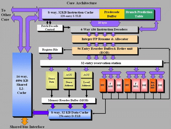
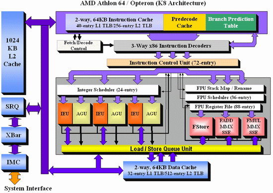
As Johan did back in the original piece, let’s start with semi-equivalent microarchitecture diagrams for Core vs. K8:


For anyone versed in x86 design, three differences immediately stand out when comparing the two. First is the reorder buffer, which for Intel ranks at 96 entries, compared to 72 for AMD. Second is the scheduler arrangement, where AMD uses split 24-entry INT and 36-entry FP schedulers from the ‘Instruction Control Unit’ whereas Intel has a 32-entry combined ‘reservation station’. Third is the number of SSE ports: Intel has three compared to two from AMD. Let’s go through these in order.
For the reorder buffers, with the right arrangement, bigger is usually better. Make it too big and it uses too much silicon and power however, so there is a fine line to balance between them. Also, the bigger the buffer it is, the less of an impact it has. The goal of the buffer is to push decoded instructions that are ready to work to the front of the queue, and make sure other instructions which are order dependent stay in their required order. By executing independent operations when they are ready, and allowing prefetch to gather data for instructions still waiting in the buffer, this allows latency and bandwidth issues to be hidden. (Large buffers are also key to simultaneous multithreading, which we’ll discuss in a bit as it is not here in Core 2 Duo.) However, when the buffer has the peak number of instructions being sent to the ports every cycle already, having a larger buffer has diminishing returns (the design has to keep adding ports instead, depending on power/silicon budget).
For the scheduler arrangements, using split or unified schedulers for FP and INT has both upsides and downsides. For split schedulers, the main benefit is entry count – in this case AMD can total 60 (24-INT + 36-FP) compared to Intel’s 32. However, a combined scheduler allows for better utilization, as ports are not shared between the split schedulers.
The SSE difference between the two architectures is exacerbated by what we’ve already discussed ? macro-op fusion. The Intel Core microarchitecture has 3 SSE units compared to two, but also it allows certain SSE packed instructions to execute within one instruction, due to fusion, rather than two. Two of the Intel’s units are symmetric, with all three sporting 128-bit execution rather than 64-bit on K8. This means that K8 requires two 64-bit instructions whereas Intel can absorb a 128-bit instruction in one go. This means Core can outperform K8 on 128-bit SSE on many different levels, and for 64-bit FP SSE, Core can do 4 DP per cycle, whereas Athlon 64 can do 3.
【对比AMD K8,酷睿2的乱序执行的优势体现在三点上,一是记录缓存96 ENTRY VS 72 ENTRY,酷睿2的前端有更高的并发,记录缓存也有4:3的优势。二是调度管理方面相比AMD拆分为24-ENTRY整型跟36-entry浮点,酷睿2为统一的32entry保留站,三是SSE执行单元数量达到三个,能够最大化利用到宏操作融合的优势,另外,酷睿2的SSE执行单元是128bit位宽,AMD只有64bit,在执行128bit SSE指令时候酷睿2有压倒性优势】

One other metric not on the diagram comes from branch prediction. Core can sustain one branch prediction per cycle, compared to one per two cycles on previous Intel microarchitectures. This was Intel matching AMD in this case, who already supported one per cycle.
Core: Load Me Up【Core架构:负载】
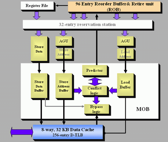
When discussing the size of the reorder buffer, I mentioned that for some ops relying on the data of others, the order in which they need to be processed has to remain consistent ? the load for the second op has to follow the store from the first in order for the calculation to be correct. This works for data that is read from and written to the same location in the same data stream, however with other operations, the memory addresses for loads and stores are not known until they pass the address generation units (AGUs).
This makes reordering a problem at a high level. You ultimately do not want a memory location to be written and stored by two different operations at the same time, or for the same memory address to be used by different ops while one of those ops is sitting in the reorder queue. When a load micro-op enters the buffer, the memory addresses of previous stores are not known until they pass the AGUs. Note, that this applies to memory addresses in the caches as well as main memory. However, if one can speed up loads and load latency in the buffers, this typically has a positive impact in most software scenarios.
With Core, Intel introduced a ‘New Memory Disambiguation’. For lack of a better analogy, this means that the issue of loads preceding stores is given a ‘do it and we’ll clean up after’ approach. Intel stated at the time that the risk that a load will load a value out of an address that is being written to by a store that has yet to be finished is pretty small (1-2%), and the chance decreases with larger caches. So by allowing loads to go head of stores, this allows a speedup but there has to be a catch net for when it goes wrong. To avoid this, a predictor is used to help. The dynamic alias predictor tries to spot this issue. If it happens, the load will have to be repeated, with a penalty of about 20-cycles.
【酷睿2强大的前端跟乱序执行带来的是更大的数据吞吐需求,Intel发现如果允许下一次载入(Load)在存储(Store)之前操作,就可以实现载入提速和降低延迟,其风险在于,存在需要载入尚待存储数据的可能(大约1~2%的几率),这时候就需要浪费20个时钟周期等待重新载入,为此,在酷睿2中加入预测器可以避免这一场景出现。】

Unofficial AnandTech Diagram
The predictor gives permission for a load to move ahead of a store, and after execution the conflict logic scans the buffer in the Memory reOrder Buffer (MOB) to detect an issue. If it happens, then the load is reprocessed back up the chain. In the worst case scenario, this might reduce performance, but as Johan said back in 2006: ‘realistically it is four steps forward and one step back, resulting in a net performance boost’.
Using this memory disambiguation technique, Intel reported a 40% performance boost purely on allowing loads to be more flexible in a number of synthetic loads (or 10-20% in real world), along with L1 and L2 performance boosts. It is worth noting that this feature affects INT workloads more often than FP workloads, purely on the basis that FP workloads tend to be more ordered by default. This is why AMD’s K8 lost ground to Intel on INT workloads, despite having a lower latency memory system and more INT resources, but stayed on track with FP.
【预测器(Predictor)允许在数据存储之前载入,同时冲突检测逻辑(Conflict logic)会扫描乱序缓冲区(Memory reorder Buffer MOB)查找问题,一旦发现立即执行重载入,在最坏的情况下性能会有所损失。根据Intel的说法性能提升幅度可以达到40%,实际执行环境中也能有10~20%的增速,在整型操作中优势尤为明显。】
Core: No Hyper-Threading, No Integrated Memory Controller【没有超线程,没有集成内存控制器】
In 2016, HT and an integrated memory controller (IMC) are now part of the fundamental x86 microarchitecture in the processors we can buy. It can be crazy to think that one of the most fundamental upticks in x86 performance in the last decade lacked these two features. At the time, Intel gave reasons for both.
Simultaneous Hyper-Threading, the act of having two threads funnel data through a single core, requires large buffers to cope with the potential doubling of data and arguably halves resources in the caches, producing more cache pressure. However, Intel gave different reasons at the time ? while SMT gave a 40% performance boost, it was only seen as a positive by Intel in server applications. Intel said that SMT makes hotspots even hotter as well, meaning that consumer devices would become power hungry and hot without any reasonable performance improvement.
On the IMC, Intel stated at the time that they had two options: an IMC, or a larger L2 cache. Which one would be better is a matter for debate, but Intel in the end went with a 4 MB L2 cache. Such a cache uses less power than an IMC, and leaving the IMC on the chipset allows for a wider support range of memory types (in this case DDR2 for consumers and FB-DIMM for servers). However, having an IMC on die improves memory latency significantly, and Intel stated that techniques such as memory disambiguation and improved prefetch logic can soak up this disparity.
【十年后的今天,超线程(HT)和内置内存控制器(IMC)是X86处理器的最基本属性,在当时,前任Pentium4引领过超线程的潮流,对手AMD则率先将内置内存控制器引入了PC领域,但酷睿2一个都没有。
同步超线程技术(Simultaneous Hyper-Threading SMT)需要在高速缓存中开出更大的缓冲区来满足多出一倍的资源的要求,酷睿2引领时代的前端设计已经是对当时工艺的极限的挑战,超线程实在是心有余而力不足,内置内存控制器AMD靠的是SOI工艺的的先天优势实现,一旦工艺允许,超线程自然会回来,内置内存控制器也不是问题,后来的nehalem不就是这么做的么?(原文以超线程优势体现在服务器上和有FB-DIMM内存为由洗地理由并不充分)相对于集成内存控制器,Intel选择了更大的L2】
As we know know, on-die IMCs are the big thing.
Core: Performance vs. Today【Core架构:今昔对比】
Looking back at Anand’s original review, and at a time where CPU performance made a lot of difference for gaming frame rates at 1600×1200, the conclusion was quite startling.
Intel’s Core 2 Extreme X6800 didn’t lose a single benchmark in our comparison; not a single one. In many cases, the $183 Core 2 Duo E6300 actually outperformed Intel’s previous champ: the Pentium Extreme Edition 965. In one day, Intel has made its entire Pentium D lineup of processors obsolete.
【在2006年,即使是最弱的E6300,都可以在很多测试中轻松放倒之前的旗舰产品Pentium XE 965,中坚产品E6600则成功击败AMD最新的旗舰产品FX-62,而旗舰产品X6800更是比E6300强了近一半。】

Imagine something like that happening today. (Actually, if you believe what we’ve been told, AMD’s upcoming AM4 platform with Zen and Bristol Ridge might make its current desktop platform obsolete, but that’s a slightly different discussion because of how integrated graphics has adjusted the landscape for CPU focused silicon somewhat.)
That’s Intel vs. Intel though, against AMD it was just as damning.
Compared to AMD’s Athlon 64 X2 the situation gets a lot more competitive, but AMD still doesn’t stand a chance. The Core 2 Extreme X6800, Core 2 Duo E6700 and E6600 were pretty consistently in the top 3 or 4 spots in each benchmark, with the E6600 offering better performance than AMD’s FX-62 flagship in the vast majority of benchmarks.
However, Core 2 Duo has now been out for 10 years. I’ve pulled up some benchmark data from our database to see if we have any matches to compare against processors that cost $214 today. The Core i5-6600 fits our bill perfectly, and there are two benchmarks which match up. I’ve also dotted the graphs with a range of more recent AMD and Intel processors for progression.
【今天的214美元产品I5-6600 VS当年同价位的E6400,十年来我们的CPU足足快了一倍,就连入门级产品G1620也轻而易举的战胜了E6400,但是不要忘记这是2.13Ghz的E6400跟一群主频接近4Ghz的产品作对比,事实上很多酷睿2用户后来升级到Sandy bridge后就再也没有换代过。】


Our 3D Particle Movement is more for idealized synthetic workloads, however FastStone is all about image conversion and favors high frequency, high single threaded performance.
Naturally, modern processors nearing 4.00 GHz have a large advantage over the 2.13 GHz version of Core 2 Duo, as well as multiple generations of improved microarchitecture designs and smaller lithography nodes for power efficiency. However, has any processor family had as much nostalgic longevity as the consumer launch of Core? One could argue that while Core put Intel on top of the heap again, Sandy Bridge was a more important shift in design and as a result, many users went from Conroe to Sandy Bridge and have stayed there.
【回顾十年前酷睿2发布后发现,在当今的skylake处理器中依旧延续了酷睿2的框架:四发射、操作融合、大容量共享高速缓存等,当然,随着工艺的进步,intel在nehalem加入了内存控制器、北桥功能和三级高速缓存,在Sandy Bridge中引入了微操作融合缓存(micro-op cache)和eDRAM,酷睿2的故事仍然没有结束。
而那个在酷睿2时代被一举拿下的对手AMD在十年间一蹶不振,K10和bulldozer麻烦不断,几乎完全退出了中高端领域的竞争,直到最近才借着新核心Zen喊出“我回来了”,然而仔细看Zen的PPT,仍然没有看到类似当年酷睿2那样石破惊天的变化,所以,AMD也许能重返中端,但论挑战似乎还很远。】
Looking to the Future:
International Technology Roadmap for Semiconductors 2.0【展望未来:国际半导体技术路线图 V2.0】
The ten year anniversary of Conroe comes at a time when the International Technology Roadmap for Semiconductors report into the next 10-15 years of the industry has been officially launched to the public. This biennial report is compiled by a group of experts in the semiconductor industry from the US, Europe and Asia and is designed to help the industry dictate which path to focus R&D for the next 10-15 years, and runs for nearly 500 pages. While we could go into extensive detail about the contents, we plan to give a brief overview here. But for people interested in the industry, it’s a great read for sure.
The report includes deep discussions regarding test equipment, process integration, radio frequency implementations (RF), microelectromechanical systems (MEMs), photolithography, factory integration, assembly, packaging, environmental issues, improving yields, modeling/simulation and emerging materials. With a focused path to a number of technologies, the hope is that leading contenders in each part of the industry can optimize and improve efficiency in directional research and development, with the possibility of collaboration, rather than taking many different routes.
【在conroe十周年纪念的日子里正值国际半导体技术路线图报告(International Technology Roadmap for Semiconductors ITRS)出炉,这份由全球各大洲的半导体工业的专家共同起草的长达500页的双年报告,是广大从业者的重要参考。报告从设备调试、工艺集成、射频(RF)、微机电(MEMS)、光刻、封装测试、改善良品率等多方面深入探讨半导体工业的未来。】
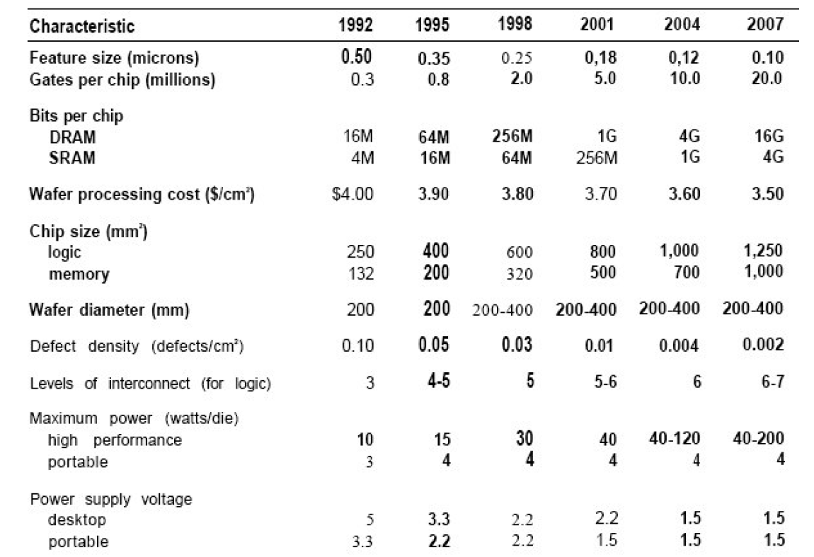
Obviously such a report is going to make successful and unsuccessful predictions, even with a group of experts, based on the introduction of moonshot style features (FinFET) or unforeseen limitations in future development. For example, here is the first roadmap published by the Semiconductor Industry Association in the first report in 1993:
【在过去,报告准确的预测过现在流行的finfet技术的流行,但也忽视过半导体的很多瓶颈,比如以下这份1993年的报告(也就是最早的报告):】

Original 1993 Semiconductor Industry Association roadmap
【1993年原版 半导体路线图】
As we can see, by 2007 it was predicted that we would be on 10nm chips with up to 20 million ‘gates’, up to 4GB of SRAM per chip and 1250mm2 of logic per die. Up to 400mm wafers were expected in this timeframe, with 200W per die and 0.002 defects per square cm (or 5.65 errors per 300mm wafer).【93年预测07年我们就能用上10nm。实际上那时Intel用的还是65nm。【实际上到10年之后的现在10nm才开始流片。】】
Compare that to 2016, where we have 16/14nm lithography nodes running 300mm wafers producing 15 billion transistors on a 610mm2 die (NVIDIA P100). Cache currently goes up to 60-65MB on the largest chips, and the power consumption of these chips (the ASIC power) is around 250W as well. So while the predictions were a little too fast on the lithography node, various predictions about the integration of components onto a base processor were missed (memory controllers, chipsets, other IO).
What makes the most recent report different is that it is listed as the last report planned by ITRS, to be replaced by a more generalized roadmap for devices and systems, the IRDS as the utility of semiconductors has changed over the last decade. In this last report, a number of predictions and focal points have been picked up by the media, indicating a true end to Moore’s Law and how to progress beyond merely shrinking lithography nodes beyond 7nm. Part of this comes from the changing landscape, the move to IoT and the demand for big data processing and storage, but also the decrease in the profitability/performance gain of decreasing node sizes in comparison to their cost to develop is, if believed, set to put a paradigm shift in integrated circuit development. This applies to processors, to mobile, to DRAM and other industry focal points, such as data centers and communications.
【实际的特征线宽的发展表面超越了1993年的预测,2001年就开始的130纳米工艺在预测中被放到了2004年,而这时候正是intel撞上了90nm大墙。互连层则落后不少,预测中2004年将采用6层互连,实际上2002年AMD消费级的Thoroughbred B处理器就用到了9层铜互连。功率问题恐怕是整个业界的始料未及,2001年40瓦的功耗早已被主频大战抛在脑后,正如本文开头所述,半导体偏离了正轨,让高功耗时代提早到来,经历过那个时代的玩家都知道,2001年的高端散热器放在2004年根本小菜一碟,因为根据长期预测,散热大规模引入热管可以等到2004年,这就是偏离的后果。
至于芯片大小方面,如果用熟知的CPU、GPU来判断的话1250平方毫米可能是天方夜谭了,毕竟就算到了今天,14/16nm时代,150亿晶体管,610平方毫米的NVIDIA P100处理器几乎到了认知极限 。但这毕竟是整个行业的报告,就拿图像传感器来说,全幅CIS的尺寸大致是864平方毫米,业界量产的时间也正好是2000~2001年,如今,索尼已经能够量产33X44幅面的传感器(面积接近1500平方毫米),所以面积一说相当准确。】
I do want to quote one part of the paper verbatim here, as it ties into the fundamental principles of the future of semiconductor engineering:
“Moore’s Law is dead, long live Moore’s Law”【“摩尔定律已死,摩尔定律万岁”】
The question of how long will Moore’s Law last has been posed an infinite number of times since the 80s and every 5-10 years publications claiming the end of Moore’s Law have appeared from the most unthinkable and yet “reputedly qualified” sources. Despite these alarmist publications the trend predicted by Moore’s Law has continued unabated for the past 50 years by morphing from one scaling method to another, where one method ended the next one took over. This concept has completely eluded the comprehension of casual observes that have mistakenly interpreted the end of one scaling method as the end of Moore’s Law. As stated before, bipolar transistors were replaced by PMOS that were replaced by NMOS that were also replaced by CMOS. Equivalent scaling succeeded Geometrical Scaling when this could not longer operate and now 3D Power Scaling is taking off.【自从上世纪80年代开始,每隔几年就会有人称摩尔定律将失效】
By 2020-25 device features will be reduces to a few nanometers and it will become practically impossible to reduce device dimensions any further. At first sight this consideration seems to prelude to the unavoidable end of the integrated circuit era but once again the creativity of scientists and engineers has devised a method ‘To snatch victory from the jaws of defeat’.
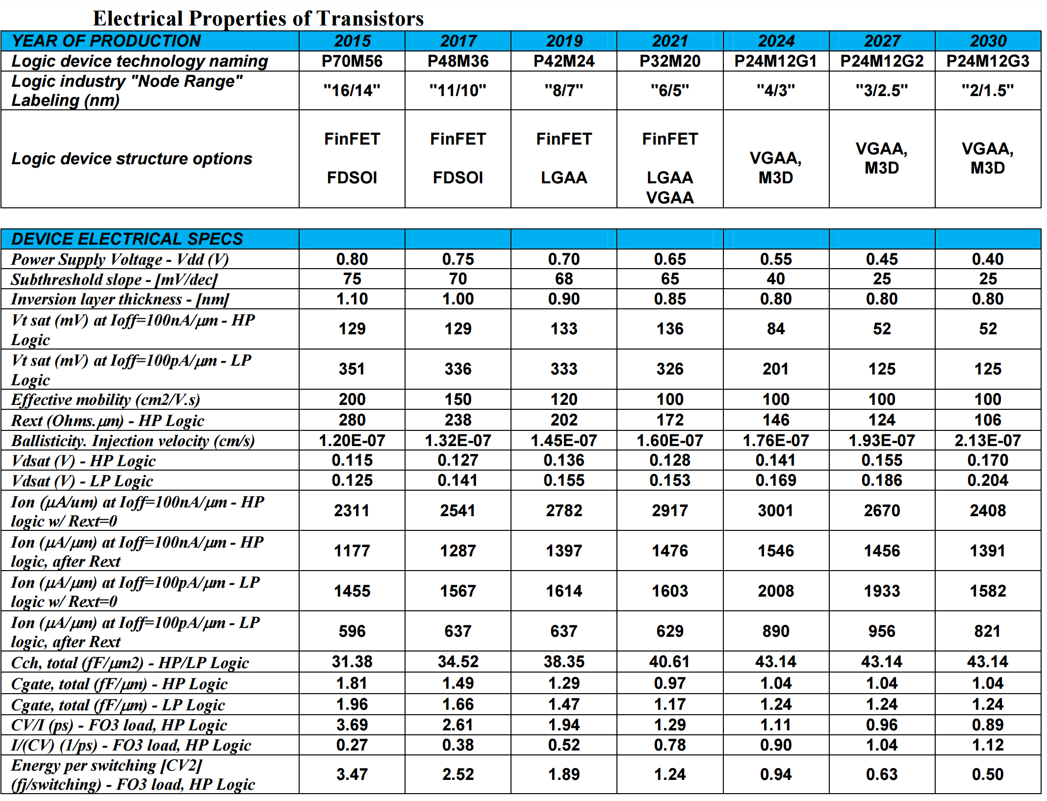
Looking To The Future: 450mm Wafers in 2021, and Down to ‘2nm’【未来:2021年,450mm晶元;以及之后的‘2nm’制程】
Most users following the industry will know that the name of the lithographic node, such as ‘14nm’, ‘16nm’ or ‘28nm’ is often an imperfect characterization of what is actually happening on the silicon. For example, Intel’s 14nm node is widely touted as the best in the industry, and the equivalent 14nm/16nm nodes are said to not be even close, due to Intel’s focus on several generations of FinFET compared to the other main semiconductor manufacturers. This also means that while ‘14nm’ or ‘16nm’ is mentioned, many other parts of the silicon could be manufactured on other nodes, depending on the utility.
【450毫米晶圆(18寸)是十年前就在讨论的概念,然而由于这十年间半导体世界被各种障碍搞得团团转,以至于更大的晶圆都被人遗忘了,此次ITRS给出了新的时间表, 2021年的DRAM工艺上会用到450毫米大晶圆,还要等五年。】
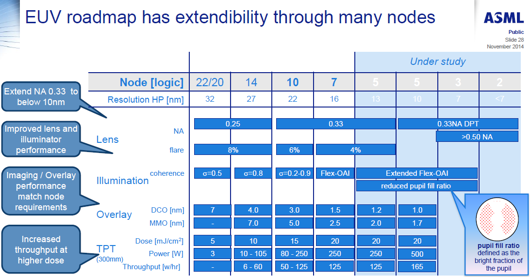
We’ve spoken in the past about equipment roadmaps to deal with the problem of shrinking lithography node sizes. This includes new lasers, droplet generation, collectors, masks, defect detection, lenses, and the technology to drive high throughput. For example, here are ASML’s EUV requirements for the next few manufacturing nodes, including requirements for 250W light sources at a 5nm node:

ASML对今后几个制程节点的EUV要求
With the ITRS report, it makes a couple of metrics regarding node sizes and wafers. On the later, we get the prediction that 450nm wafers should be in play at around 2021 for DRAM:
【到了2021年,DRAM的核心面积将缩小到780平方纳米,当今的数字为3480,2021将是最后的finfet(鳍式场效应晶体管),在2030年会看到2nm工艺。】

This matches at DRAM half-pitch of 15nm, or a DRAM cell size of 780nm2, compared to 3480nm2 today. The movement to 450mm wafers has been expected for some time, with early predictions going for the 2008-2011 timeframe, however development seems to have stalled for a variety of reasons.
When it comes to transistors, given the node naming scheme caveats listed above, the ITRS report predicts that FinFET will make way at around the 2021 timeframe in favor of 3D stacking such as ‘vertical gate all-around’ (VGAA). As the node shrinks, as well as the transistor size, the power supply voltage will drop from 800mV today down to 400/450mV by 2027.
【今天的当红小生Finfet还有5年的发展期,进入7nm的时间表是2019年,2021年在5nm上终结。让Athlon64大红大紫的SOI工艺(绝缘体上硅)则会在2017年终结,末代皇帝将是10nm FDSOI,取代Finfet的将是VGAA(vertical gate all-around),2021年登场,预计会在2030年进入2nm制程,这时候的核心电压仅为0.4V。制程的未来之路是坎坷的,5nm以后会怎样仍然有很大变数。2021年可能从FinFET转向VGAA】

Moving into a world of IoT will require even lower power transistors, of which moving to a ‘smaller node’ and vertical chip integration will be a large part.
The ITRS report goes into a lot of detail regarding different stacking technologies, such as the 2.5D integration we see on products like AMD’s Fiji GPU involving a silicon interposer, as well as 3D and the different ways to implement both microchannel cooling in such chips as well as 3D TSV applications.
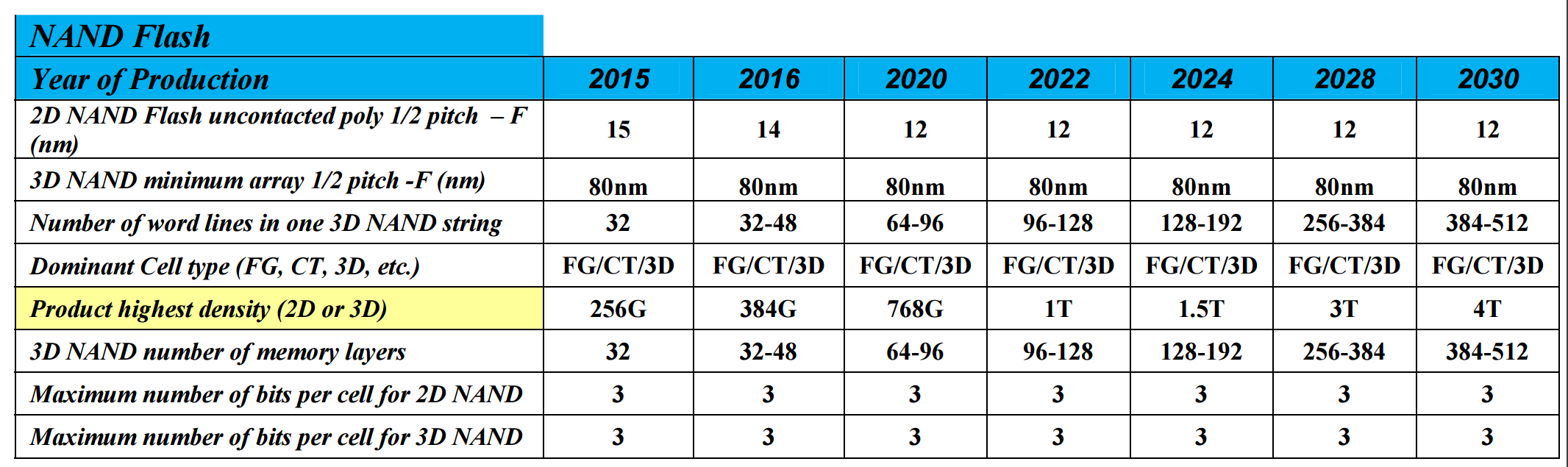
Looking To The Future: NAND Flash Scales Up to 64 TB SSDs in 2030【未来:2030年会有64TB SSD】
Over the past few years, the NAND Flash industry has gone through two major shifts in technology: the movement from 1 to 2 to 3 bits per cell, which directly increases bit density and capacity, and also moving from planar flash to variants of 3D stacking. Stacking can refer to individual NAND dies, as well as stacking those dies into a single package: both of these features are being extensively investigated to increase density also. There are two main drivers for this: reduction in cost, and capacity. However, despite this, the predictions in the ITRS report for NAND flash are primarily looking at improvements to numbers of layers rather than lithography changes or moving to more bits per cell.

As we can see, TLC (according to the report) is here to stay. QLC, or whatever you want to call it, is not mentioned. The two changes are the number of memory layers, moving from 32 today to 128 around 2022 and then 256/512 by 2030, and the number of word-lines in one 3D NAND string. This gives a product density projection of 256 Gbit packages today to 1 Tbit packages in 2022 and 4 Tbit packages in 2030.
If we apply this to consumer drives available today, we can extrapolate potential SSD sizes for the future. The current Samsung 850 EVO 4 TB uses Samsung’s 48-layer third generation V-NAND to provide 256 Gbit TLC parts. Alongside the 4 TB of memory, the controller requires 4 GB of DRAM, which is another concern to remember. So despite the report stating 256 Gbit in 32-layer, we have 256 Gbit in 48-layer, which is a difference primarily in die-size predictions for the report. Still, if we go off of the product density we should see 12 TB SSDs by 2020, 16 TB in 2022, 48 TB in 2028 and 64 TB drives in 2030. It’s worth noting that the ITRS report doesn’t mention power consumption in this table, nor controller developments which may be a substantial source of performance and/or capacity implementations.
【NAND闪存,大家不要慌,不会有什么QLC了,前些年在刚引入TLC NAND(3bit)的时候业界还在预测QLC(4bit)的存在,经过这些年的发展可能业界自己对QLC的可行性已经失去信心,毕竟TLC已经是毒瘤般的表现,于是ITRS的预测中完全没有看到QLC的存在,万幸。
未来NAND仍然得靠3D堆叠来实现扩容,当前单封装密度为三星850EVO上48层堆叠的256Gbit,到了2022年可以达到128层1Tbit,2030年到512层4Tbit,这时候就会看到64TB的SSD了。】
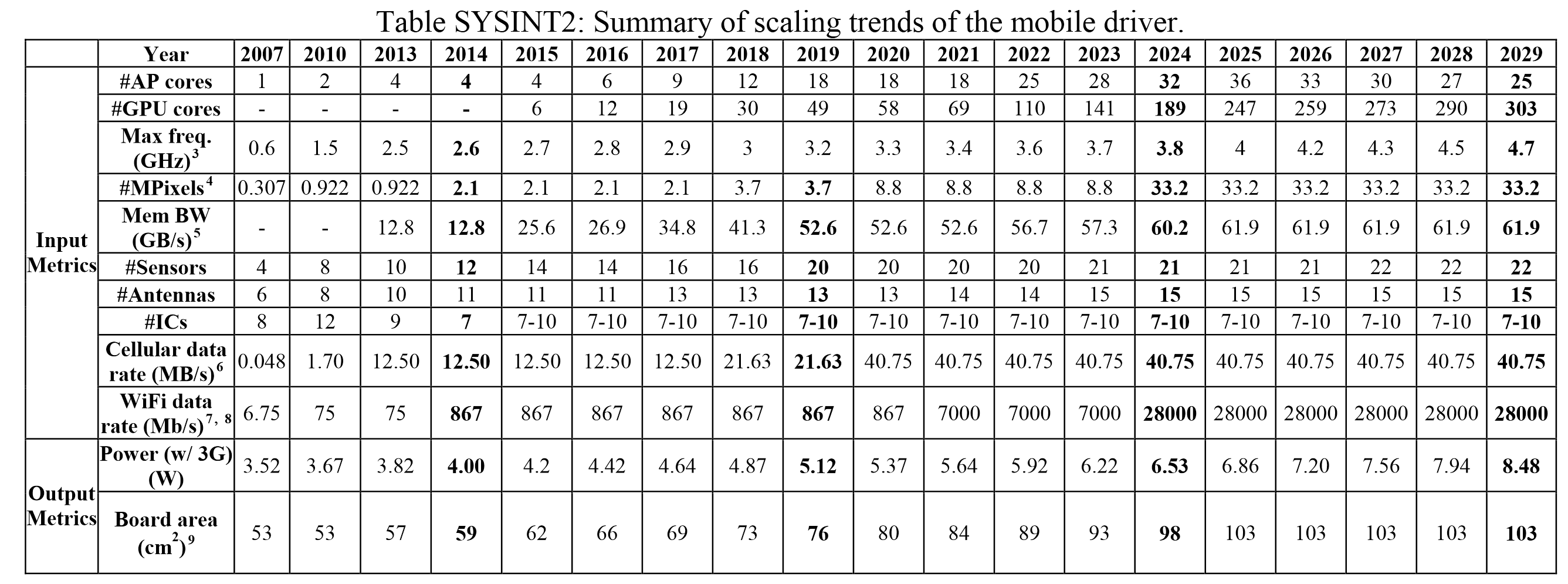
Looking To The Future: Mobile, 32-cores and 8K Displays【未来:32核手机处理器,8K显示屏】
The volume of the mobile industry today is certainly a hot topic, especially with Intel scrapping their mobile platform as recently as April 2016. This primarily leaves ARM (who was recently acquired by Softbank) in the driving seat for providing the next decade of mobile processor designs. Because ARM sells licences, both processor licences and architecture licences, a number of ARM’s partners have taken the base instructions and decided to forgo ARM’s core designs for their own. This is why we currently see Samsung with their M1 core, Qualcomm with their Kryo core, and Apple with their Twister cores as well, while Huawei, Mediatek and others are combining parts of ARM’s core designs with various GPU designs either from ARM or Imagination. Getting the right combination of parts, as well as the industrial design, are key elements to the user experience as well as the mobile industry as a whole.
Then of course, Mediatek announced the Helio X20 last year, which is finally now in devices. This is a 10-core part, using a paradigm such that the most relevant cores needed for performance and power consumption are in play at the right time. The creation of a 10-core part made a number of industry analysts wonder which direction this market was going in, as on the one end we have the Helio X20, while Apple’s latest iPhone family were using dual-core designs of Apple’s custom implementation. So if 10-cores are too much, this roadmap might come a little surprising.

As we stand in 2016, this roadmap states we are currently in a 6-core mobile CPU arrangement with 12 GPU cores, with the CPU running at 2.8 GHz. Displays are around the Full-HD mark, with overall board power at 4.42W. Well we certainly have hex-core parts today (2xA57 + 4xA53), 12-core GPUs also exist in Apple’s products, and Samsung’s M1 core is rated at 2.8 GHz. Some phones, such as Sony’s Xperia Z5 Premium, already have 4K screens (8.3MP), which is more geared towards 2020 in this roadmap.
【ITRS对手持平台的预测是基于当前手机SOC蓬勃发展的,2016年6核CPU 12核GPU,26.9Gbps内存带宽,4.42瓦功耗的数据实际已经开始偏离效率,从2014年开始手机SOC对先进工艺的渴望就赶上了台式机CPU,以至于近年台积电不断表示10nm要比intel早,intel也毫不在乎。到2019年也许还能看到18核3.2Ghz,49GPU核心的怪物,但2024年真能看到3.8Ghz 32核CPU 189核GPU轻松实现8K应用的怪物么?值得怀疑,毕竟今天的表现都已经是对当前工艺的深度榨取。】
Cycle now from 2016 to 2025, almost 10 years in the future. ITRS’ roadmap states the following:【到2025年的预计】
- 36-cores【36核心】
- 247 GPU cores【247个GPU核心】
- 4.0 GHz【4GHz主频】
- 8K Screens (33.2 MP)【8K显示屏】
- 61.9 GB/s memory bandwidth【61.9GB/S内存带宽】
- 28 Gbit/s WiFi【28Gb/s的WIFI带宽】
- 6.86W Board Power【功耗6.86W】
- 103 cm2 board area【芯片面积103cm2】
Now clearly, for this piece I conferred with our mobile team and I got a lot of confused faces. Even scaling down from 16nm in 2016 to 4nm in 2025, they felt that so many all-purpose cores in a chip (as well as all the GPU cores) was probably excessive, not only in terms of utility but also for 2D floor plan. In order to implement this, more z-height would be needed as well as appropriate 3D technologies in place. Andrei felt the frequency targets were more respectable, and the memory bandwidth would depend on how the silicon designers decided to implement on-package DRAM vs multi-channel implementations. The board power seemed a little excessive, if only because the laws of physics can’t change that drastically, and an increase in +50% board area just means a bigger device.【即使2025年能达成4nm制程,在移动设备里塞进那么多CPU、GPU核心也有点太激进。2D平面结构的限制已经开始展现,Z轴上的空间应该要开始发挥作用,即3D技术】
Looking To The Future
While today is Conroe’s 10 year anniversary, I was a post-teenage system builder when it was first released. Now, as AnandTech’s CPU editor, it has been fun for me to delve back into the past and revisit some of the fundamental design changes that would steer a significant amount of Intel’s future design. You can certainly feel many of the technologies used in the Core microarchitecture in Skylake today, including operation fusion and large shared caching. Now of course, a number of technologies have been developed since which make a big difference too, such as micro-op caches from Sandy Bridge, an L3 cache, even adaptations for eDRAM and moving the memory controller and north bridge on-die. But it does make me wonder if there will be another Intel microarchitecture as important as this down the line. On the AMD side of the fence, everyone is looking at Zen with wide eyes and anticipation. While we have been told not to expect it to take the performance crown, a number of users and industry analysts hope that it brings more competition to the x86 space, enough to rekindle the competitive spirit in silicon back in the mid-2000s.
Looking into the International Technology Roadmap for Semiconductors report, and even just the 50-page summary, there are a large number of predictions in the industry that could happen. There are thousands of people working to make sure the next process node, and the one after that, happens with good yields and on time. The report goes into detail about how shrinking that process won’t happen forever, which is a sentiment that the industry has had for a while, and it lays out in a series of working groups what needs to happen at each stage of the process to go beyond Moore’s Law, specifically regarding silicon stacking, TSVs, and the movement to 3D chips. The ITRS report is set to be the last, with the new focus on devices, systems, SiP and other technologies beyond Moore’s Law. Some have heralded the lack of a future ITRS report as a stark warning, however the fact that we can’t keep shrinking forever has been a known fact, especially at the point where most businesses won’t shrink a process node unless it can net them an overall profit. The movement to 3D makes everything a lot more complicated, but it has to happen in order to provide semiconductor growth and improvements beyond 2D.
【传统意义上的摩尔定律早已消亡,但在今年的ITRS报告中依旧可以清楚的看到摩尔定律的影子,尤其是那张移动SOC的发展路线图,乐观程度堪比没有撞上90nm大墙时候的intel,这就是所谓的永生吧。】
Sources
Johan’s Conroe vs K8 Architecture Deep Dive, 2006
Anand’s Core 2 Extreme and Core 2 Duo Review, 2006
International Technology Roadmap for Semiconductors 2.0 Report, 2015/2016
233