【AMD Zen 微架构解析 Part1:双调度器,微指令缓存以及缓存架构】AMD Zen Microarchitecture: Dual Schedulers, Micro-Op Cache and Memory Hierarchy Revealed
source:http://www.anandtech.com/show/10578/amd-zen-microarchitecture-dual-schedulers-micro-op-cache-memory-hierarchy-revealed
自翻,转载请注明出处。

In their own side event this week, AMD invited select members of the press and analysts to come and discuss the next layer of Zen details. In this piece, we’re discussing the microarchitecture announcements that were made, as well as a look to see how this compares to previous generations of AMD core designs.
【AMD这边邀请了部分媒体和分析师参与Zen的进一步细节的讨论。这篇文章里我们将讨论架构,并与前代处理器作比较。】
AMD Zen
Prediction, Decode, Queues and Execution【分支预测、解码、队列以及执行】
First up, let’s dive right into the block diagram as shown:
【首先让我们之间看下面的图】

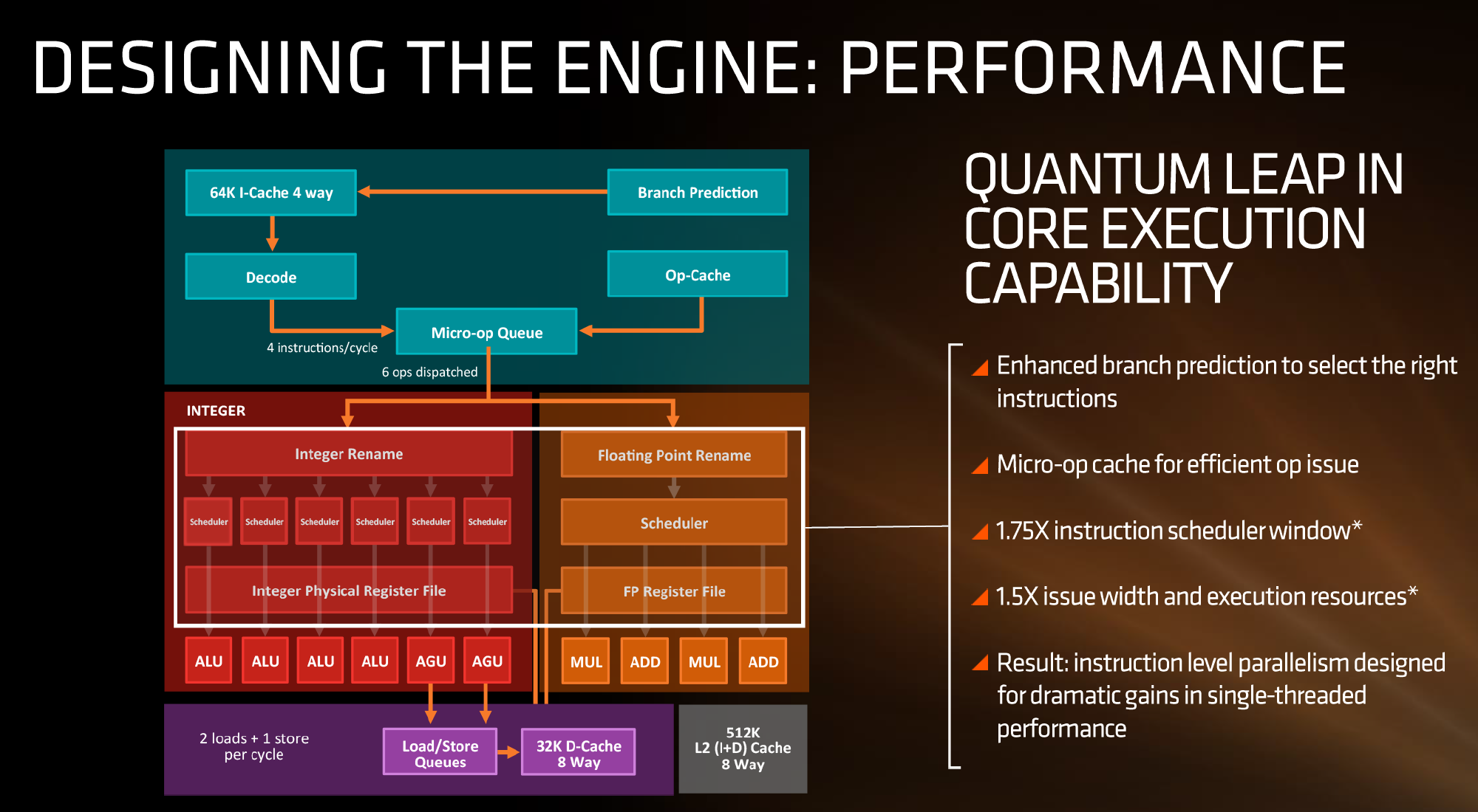
If we focus purely on the left to start, we can see most of the high-level microarchitecture details including basic caches, the new inclusion of an op-cache, some details about decoders and dispatch, scheduler arrangements, execution ports and load/store arrangements. A number of slides later in the presentation talk about cache bandwidth.
【如果我们从左边开始看起,我们可以看到大部分的架构细节,包括L1缓存、新的微指令缓存、解码、分发、调度器、执行端口以及L/S单元的设计。】

Firstly, one of the bigger deviations from previous AMD microarchitecture designs is the presence of a micro-op cache (it might be worth noting that these slides sometimes say op when it means micro-op, creating a little confusion). AMD’s Bulldozer design did not have an operation cache, requiring it to fetch details from other caches to implement frequently used micro-ops. Intel has been implementing a similar arrangement for several generations to great effect (some put it as a major stepping stone for Conroe), so to see one here is quite promising for AMD. We weren’t told the scale or extent of this buffer, and AMD will perhaps give that information in due course.
【首先,Zen与前代架构的很大一处不同在于,出现了微指令缓存(ppt上有时候写的op缓存,实际上意思就是micro-op,容易误导人)。AMD的推土机设计没有微指令缓存,就必须从其他缓存中提取细节,来执行频繁使用的微指令。Intel很早就开始用微指令缓存了,效果非常好(在Conroe架构上引入的重要改进),所以对于AMD来说这应该能带来不小提升。AMD没告诉我们这个缓冲区的大小,估计在适当的时候会给出信息。】
Aside from the as-expected ‘branch predictor enhancements’, which are as vague as they sound, AMD has not disclosed the decoder arrangements in Zen at this time, but has listed that they can decode four instructions per cycle to feed into the operations queue. This queue, with the help of the op-cache, can deliver 6 ops/cycle to the schedulers. The reasons behind the queue being able to dispatch more per cycle is if the decoder can supply an instruction which then falls into two micro-ops (which makes the instruction vs micro-op definitions even muddier). Nevertheless, this micro-op queue helps feed the separate integer and floating point segments of the CPU. Unlike Intel who uses a combined scheduler for INT/FP, AMD’s diagram suggests that they will remain separate with their own schedulers at this time.
【抛开含糊不清的“增强的分支预测器”,AMD这次也没披露解码器的设计,但列出他们每周期可以解码4条指令到队列。这个队列在微指令缓存的辅助下,到调度器时能达到最高每周期6条指令。因为解码器可以解码一条指令,然后该指令随后拆分为两条微指令(这让指令和微指令的区别变得模糊)。此外,这个微指令队列还能提高每个整数和浮点单元的利用率。AMD不像Intel那样给整数/浮点一个公用的调度器,而是继续使用分离的调度器。】
The INT side of the core will funnel the ALU operations as well as the AGU/load and store ops. The load/store units can perform 2 16-Byte loads and one 16-Byte store per cycle, making use of the 32 KB 8-way set associative write-back L1 Data cache. AMD has explicitly made this a write back cache rather than the write through cache we saw in Bulldozer that was a source of a lot of idle time in particular code paths. AMD is also stating that the load/stores will have lower latency within the caches, but has not explained to what extent they have improved.
【整数部分包括ALU、AGU以及LS操作。LS单元每周期可以执行2次16字节的load以及1次16字节的store操作,利用32KB 8路组相连 回写式L1数据缓存。AMD明确说明这是回写式缓存,而不是推土机上的穿透式缓存(在一定条件下会带来大量的闲置时间)。AMD声称缓存内的LS操作延迟会更低,但没再做进一步说明。】
The FP side of the core will afford two multiply ports and two ADD ports, which should allow for two joined FMAC operations or one 256-bit AVX per cycle. The combination of the INT and FP segments means that AMD is going for a wide core and looking to exploit a significant amount of instruction level parallelism. How much it will be able to depends on the caches and the reorder buffers ? no real data on the buffers has been given at this time, except that the cores will have a +75% bigger instruction scheduler window for ordering operations and a +50% wider issue width for potential throughput. The wider cores, all other things being sufficient, will also allow AMD’s implementation of simultaneous multithreading to potentially take advantage of multiple threads with a linear and naturally low IPC.
【每核心浮点部分包括两个乘法端口,两个ADD端口,每周期能够执行两条捆绑的FMAC命令或者一条256bit AVX。把整数和浮点部分合起来看,Zen核心在指令级并行上将会有很大提升 – 提升多少取决于缓存和重排序缓存 – 这次没给出ROB的具体数据,只说排序操作的指令调度窗口将会增大75%,发射宽度提升50%。即便是天生IPC就低的AMD处理器,核心并行性越好,其他的方面就有效率多了,这也使得这次用的SMT在多线程上占得先机。】
Deciphering the New Cache Hierarchy
【解密新的缓存结构】

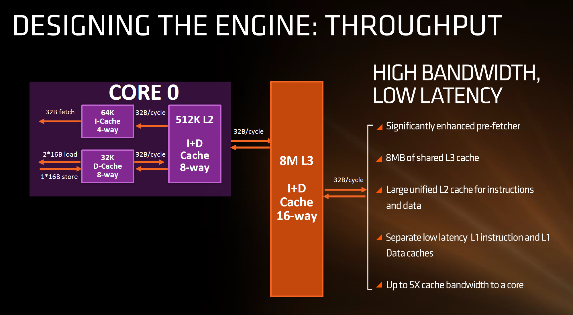
The cache hierarchy is a significant deviation from recent previous AMD designs, and most likely to its advantage. The L1 data cache is both double in size and increased in associativity compared to Bulldozer, as well as being write-back rather than write-through. It also uses an asymmetric load/store implementation, identifying that loads happen more often than stores in the critical paths of most work flows. The instruction cache is no longer shared between two cores as well as doubling in associativity, which should decrease the proportion of cache misses. AMD states that both the L1-D and L1-I are low latency, with details to come.
【这次的缓存结构相比以前做出了重大改进,而且是朝着好的方向。相较于推土机,Zen的L1缓存在大小和关联性都翻倍了,而且是写回式而不是穿透式。同时采用了非对称LS单元,因为在大多数情况下Load操作比Store要频繁得多。指令缓存不再是两个核心共享,同时关联性也翻倍,这将减少缓存未命中的情况。AMD声称L1数据和指令缓存延迟都很低,今后将公布更多细节。】
The L2 cache sits at half a megabyte per core with 8-way associativity, which is double that of Intel’s Skylake which has 256 KB/core and is only 4-way. On the other hand, Intel’s L3/LLC on their high-end Skylake SKUs is at 2 MB/core or 8 MB/CPU, whereas Zen will feature 1 MB/core and both are at 16-way associativity.
【L2缓存变成了每核心512KB,8路相连,这是Intel Skylake上256kb 4路关联的两倍。另一方面,Intel的L3在高端Skylake i7上是每核心2MB,每CPU8MB,在Zen上则是每核心1MB,这两者都是16路关联。】
Edit 7:18am: Actually, the slide above is being slightly evasive in its description. It doesn’t say how many cores the L3 cache is stretched over, or if there is a common LLC between all cores in the chip. However, we have recieved information from a source (which can’t be confirmed via public AMD documents) that states that Zen will feature two sets of 8MB L3 cache between two groups of four cores each, giving 16 MB of L3 total. This would means 2 MB/core, but it also implies that there is no last-level unified cache in silicon across all cores, which Intel has. The reasons behind something like this is typically to do with modularity, and being able to scale a core design from low core counts to high core counts. But it would still leave a Zen core with the same L3 cache per core as Intel.
【实际上上面的ppt在描述上有点暧昧。没有说多少核心共享8M L3,更没说是否每颗芯片上的所有核心都是共享同一个L3的。然而我们从一个消息来源获得的信息(在AMD官方ppt上找不到的)表明,Zen的8核芯片上是4个核心为一个簇,每个簇4个核心共享8M L3,8核芯片有两组8MB,共16MB的 L3。这样的话就是每核心2MB,但这也说明了Zen的L3不是完全共享的,然而Intel的是完全共享的。这样做的原因估计和模块化有点关系,通过增加这样的模块可以做出从4核心直到32核心,但Zen的每核心L3和Intel的依然都是每核心2MB(没有任何优势)】

What this means, between the L2 and the L3, is that AMD is putting more lower level cache nearer the core than Intel, and as it is low level it becomes separate to each core which can potentially improve single thread performance. The downside of bigger and lower (but separate) caches is how each of the cores will perform snoop in each other’s large caches to ensure clean data is being passed around and that old data in L3 is not out-of-date. AMD’s big headline number overall is that Zen will offer up to 5x cache bandwidth to a core over previous designs.
【这也意味着,AMD的L1和L2比Intel更大、延迟更低。而且L1、L2距离核心更近,还是每核心独立的,在单线程性能上会有显著提升。但更大的独立L1/L2带来的坏处是,每个核心都要监听其他核心的缓存,确保 1.传递的是干净数据、2. L3上的原数据不过期。AMD给出的总体数字是,Zen在缓存带宽上是前代的5倍。】
Low Power, FinFET and Clock Gating
【低功耗,FinFET,门控时钟】
When AMD launched Carrizo and Bristol Ridge for notebooks, one of the big stories was how AMD had implemented a number of techniques to improve power consumption and subsequently increase efficiency. A number of those lessons have come through with Zen, as well as a few new aspects in play due to the lithography.
【在AMD发布Carrizo和Bristol Ridge的时候,介绍的一个重点就是一系列降低功耗和提升能效的技术。有一部分技术延续到了Zen上,同时伴随着制程更新,还加入了一些新的技术。】

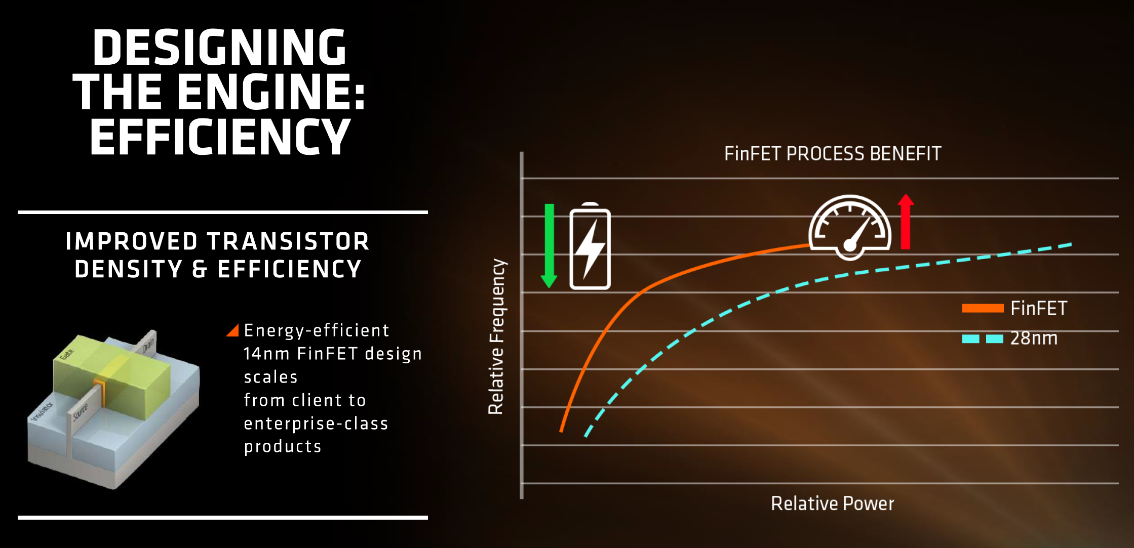
First up is the FinFET effect. Regular readers of AnandTech and those that follow the industry will already be bored to death with FinFET, but the design allows for a lower power version of a transistor at a given frequency. Now of course everyone using FinFET can have a different implementation which gives specific power/performance characteristics, but Zen on the 14nm FinFET process at Global Foundries is already a known quantity with AMD’s Polaris GPUs which are built similarly. The combination of FinFET with the fact that AMD confirmed that they will be using the density-optimised version of 14nm FinFET (which will allow for smaller die sizes and more reasonable efficiency points) also contributes to a shift of either higher performance at the same power or the same performance at lower power.
【首先就是FinFET。虽然大部分的人都已经熟悉FinFET到吐了,但我们还是要介绍一下。FinFET设计能在给定频率下设计出晶体管的低功耗版本。每个FinFET代工厂给出的技术指标都不同,但Zen用的GF 14nm技术和Polaris GPU的不会差太多,这意味着AMD使用的是14nm的追求密度版本,能在同等功耗下达成更高性能,或者低功耗下达成同等性能。】
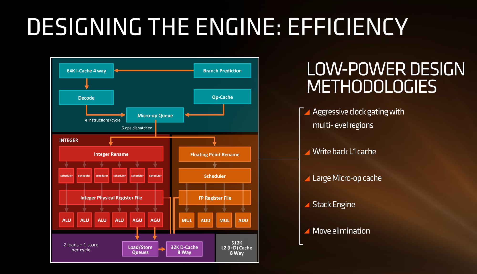
AMD stated in the brief that power consumption and efficiency was constantly drilled into the engineers, and as explained in previous briefings, there ends up being a tradeoff between performance and efficiency about what can be done for a number of elements of the core (e.g. 1% performance might cost 2% efficiency). For Zen, the micro-op cache will save power by not having to go further out to get instruction data, improved prefetch and a couple of other features such as move elimination will also reduce the work, but AMD also states that cores will be aggressively clock gated to improve efficiency.
【AMD介绍说工程师们一直很注重功耗和能效,在性能和功能单元的效率上做了很多权衡(比如提升1%的性能,代价是2%的能效损失)。不仅有微指令缓存可以节约读取指令缓存的电能,改善的预取机制等也能减少工作量。但AMD也说明,为了提升能效,Zen的门控时钟将会很激进。】
We saw with AMD’s 7th Gen APUs that power gating was also a target with that design, especially when remaining at the best efficiency point (given specific performance) is usually the best policy. The way the diagram above is laid out would seem to suggest that different parts of the core could independently be clock gated depending on use (e.g. decode vs FP ports), although we were not able to confirm if this is the case. It also relies on having very quick (1-2 cycle) clock gating implementations, and note that clock gating is different to power-gating, which is harder to implement.
【AMD第七代APU上也有差不多的设计,保持在效率最高的那个点(特定性能)是最好的方式。上图似乎暗示着每个核心的不同部分(取决于用途)都有独立的门控时钟(比如解码单元或者浮点端口),虽然目前还无法确认。同时还需要有非常快速的门控时钟(1-2个周期),要知道门控时钟与功耗门限不同,门控时钟更难设计。】
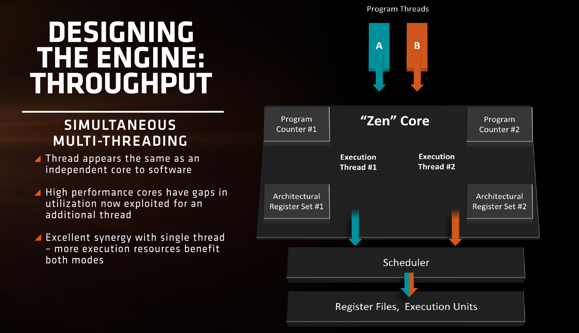
Simultaneous Multi-Threading【同步多线程】
On Zen, each core will be able to support two threads in what is called ‘simulatenous multi-threading’. Intel has supported their version of SMT for a number of years, and other CPU manufacturers like IBM support up to 8 threads per core on their POWER8 platform designs. Building a core to be able to use multiple threads can be tough, as it requires a lot of resources to make sure that the threads do not block each other by consuming all the cache and buffers in play. But AMD will equip Zen with SMT which means we will see 8C/16T parts hitting the market.
【Zen架构上,每个核心支持两个线程,这叫做同步多线程。Intel版本的SMT早在08年就开始启用,其他的厂商比如IBM,在POWER8上支持最多8个线程(SMT8)。让一个核心处理两个线程很困难,需要很多资源来确保线程之间不会因争夺缓存而互相阻塞。Zen桌面版将会有8核16线程。】

Unlike Bulldozer, where having a shared FP unit between two threads was an issue for floating point performance, Zen’s design is more akin to Intel’s in that each thread will appear as an independent core and there is not that resource limitation that BD had. With sufficient resources, SMT will allow the core instructions per clock to improve, however it will be interesting to see what workloads will benefit and which ones will not.
【在推土机上,共享浮点单元使得浮点性能不如人意。但Zen的设计更类似于Intel,每个线程都和一个单独核心差不多,不会有推土机上的资源限制。有了更多的资源,SMT将会提升IPC,我很想看看哪些负载能从中获益。】
Timeframe and Availability【时间表、供货日期】
At the presentation, it was given that Zen will be available in volume in 2017. As the AM4 platform will share a socket with Bristol Ridge, users are likely to see Bristol Ridge systems from AMD’s main OEM partners, like Dell and others, enter the market before separate Zen CPUs will hit the market for DIY builders. It’s a matter of principle that almost no consumer focused semiconductor company releases a product for the sale season, and Q1 features such events as CES, which gives a pretty clear indication of when we can expect to get our hands on one.
【在ppt上写着Zen将会在17年大量出货。由于AM4平台上Summit Ridge和Bristol Ridge使用同样的插槽,可能我们能从AMD的OEM们那里先见到Bristol Ridge进入市场。没有哪个主卖消费级产品的半导体厂商会在年末清仓季发布新品,而第一季度会有CES之类的大型展会,那时候我们肯定能拿到手。】
It’s worth noting that AMD said that as we get closer to launch, further details will come as well as deeper information about the design. It was also mentioned that the marketing strategy is also currently being determined, such that Zen may not actually be the retail product name for the line of processors (we already have Summit Ridge as the platform codename, but that could change for retail as well).
【AMD说距离发布越近,就会公布越多的架构细节。还提到了营销策略上的决定,比如Zen不会是实际产品线的名称(实际平台代号是Summit Ridge,但到了出货时候也可能会变)。】

Wrap Up【总结】
AMD has gone much further into their core design than I expected this week. When we were told we had a briefing, and there were 200-odd press and analysts in the room, I was expecting to hear some high level puff about the brand and a reiteration of their commitment to the high end. To actually get some slides detailing parts of the microarchitecture, even at a basic cache level, was quite surprising and it somewhat means that AMD might have stolen the show with the news this week.
【这次AMD的介绍比我想的要深入。当有人告诉我去参加一个短会,并且会有200多家媒体和分析师到场,我还估计应该就是吹吹牛逼,重申要回到高端市场什么的。但实际上AMD给出了部分架构的详尽介绍,甚至还介绍了基本缓存结构,这出乎我的意料,估计这个星期媒体上都会是AMD的新闻了吧。】
请支持独立网站,转发请注明本文链接:http://www.moepc.net/?post=385