【AMD进一步揭晓Zen架构细节 – 性能在Excavator基础上大幅提升,超强吞吐量】AMD Opens The Lid on Zen Architectural Details at Hot Chips ? Huge Performance Leap Over Excavator, Massive Throughput on 14nm FinFET Design
source:http://wccftech.com/amd-zen-architecture-hot-chips/
本译文未经许可不得转载,严禁私自篡改标题、内容以及二次投递。
请支持独立网站,转发请注明本文链接:http://www.moepc.net/?post=397
相关文章:AMD Zen 微架构完全解析:双调度器,微指令缓存以及缓存架构
AMD has presented tons of more information on their upcoming Zen architecture at Hot Chips. Expected to launch later this year, the Zen architecture focuses on three key departments, performance, throughput and efficiency. With Zen, AMD plans to come back to the performance CPU sector with a bang in the mainstream and enthusiast market.
【AMD在Hot Chips大会上展示了成吨的Zen架构细节。明年发布的Zen将专注于性能、吞吐量和能效的改善。凭借着Zen架构,AMD计划重返性能级CPU行列,冲击主流和发烧市场。】
AMD Zen Architecture Fully Detailed ? Wider, High-Performance and Efficient Core Design
【Zen架构完全解密 – 高并行度、高性能、高效率的核心设计】
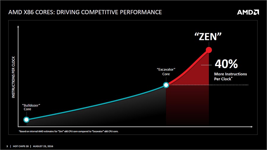
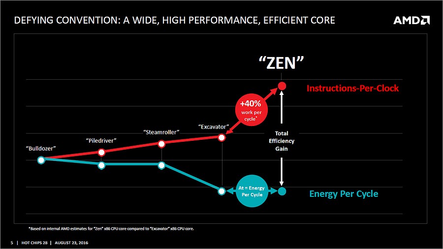
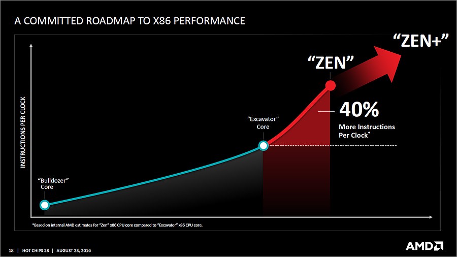
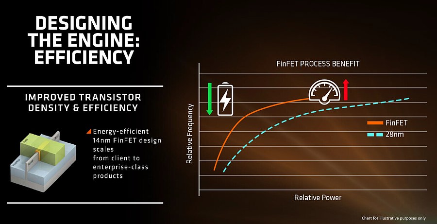
To start off with the details, Zen is based on the latest 14nm FinFET node. The only two foundries that have this node are Global Foundries and Samsung but we suspect AMD is using the former to develop Zen chips. The Zen core is said to feature 40% more instructions per clock compared to Excavator core.
【Zen基于GF 14nm FinFET制程,IPC相比Excavator提升了40%。】
AMD’s full Zen Hot Chips presentation reveals complete architecture details.
【AMD在Hot Chips上的PPT揭露了完整的Zen架构细节】
Excavator core is featured on AMD’s Carrizo and Godavari processors. The large jump in IPC would help AMD achieve performance parity with Intel chips. In fact, AMD already demoed a 8 core Summit Ridge CPU based on Zen against a Broadwell-E 8 core chip. The demo showed AMD’s solution having better rendering performance than Intel’s HEDT solution.
【相比Carrizo和Godavari上的Excavator核心,大幅提升了IPC的Zen核心将会带来与Intel比肩的性能。实际上之前的渲染演示中,Zen已经比Brodwell-E 8核要略好了。】
AMD Zen Core Design and Core Engine
【Zen核心设计】
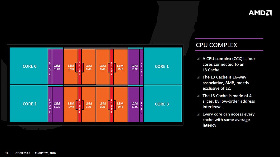
The basic building block of Zen is the core complex. The core complex comprises of four cores connected to an L3 cache. The L3 cache is 16-Way associated and makes up a total of 8 MB (mostly exclusive of L2 cache). The L3 cache is sliced into four, each comprising of two 1 MB L3 sub-slices. All cores can access these cache blocks with the same average latency speed.
【Zen的基本架构单元为CPU COMPLEX(CCX)。一个CCX内有4个核心,连接到同一块L3上。L3为16路关联,总共8MB容量,被分为4个区片,每个区片都有2片1MB的子区片,每个核心到达这些子区片的延迟都相同。】
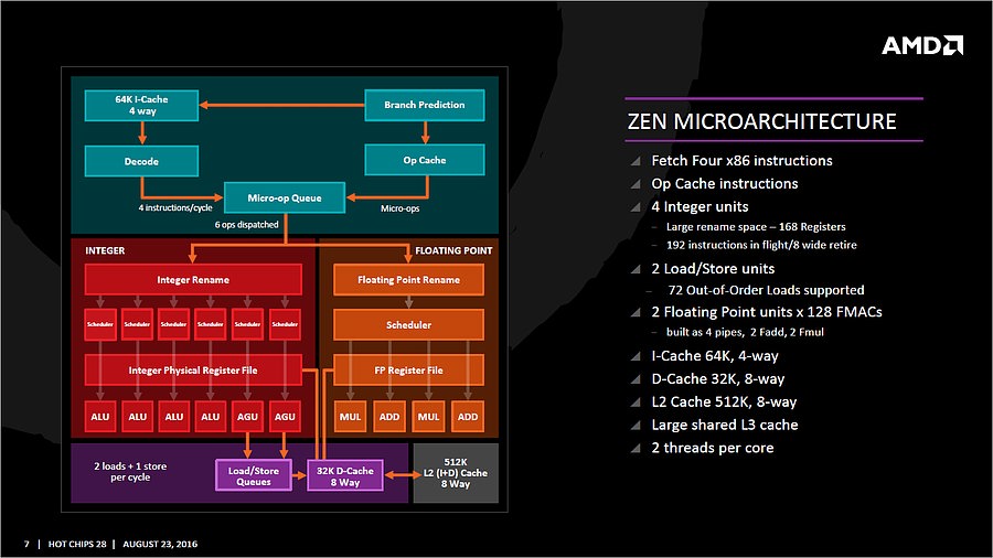
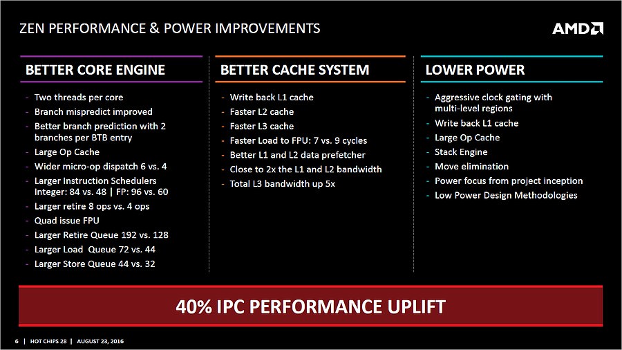
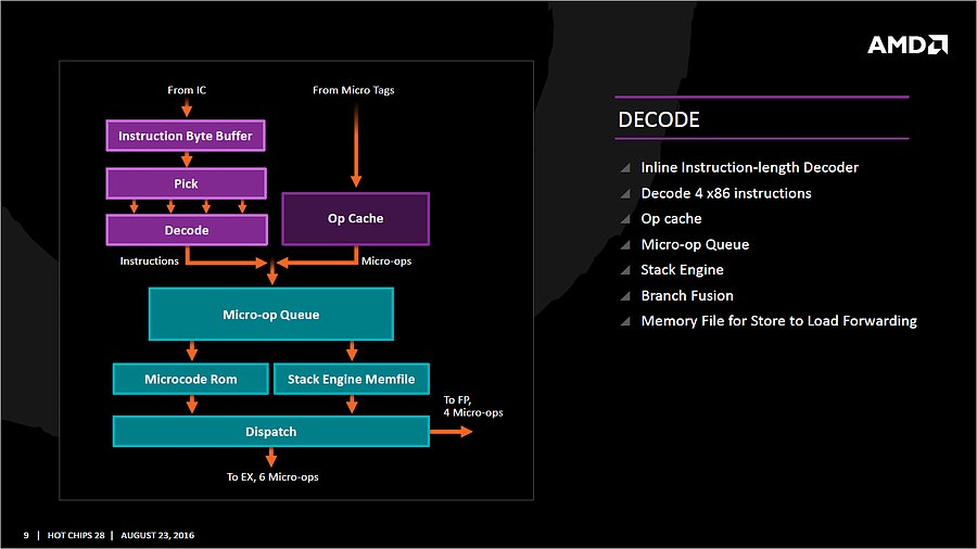
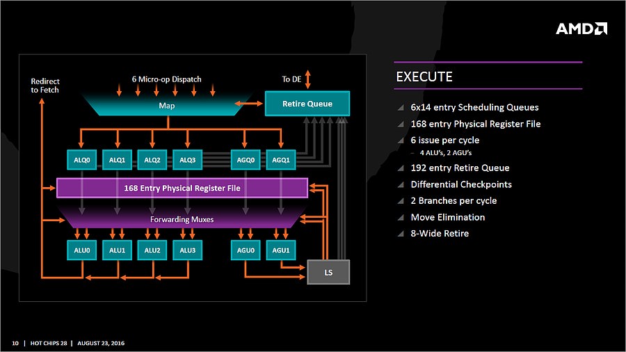
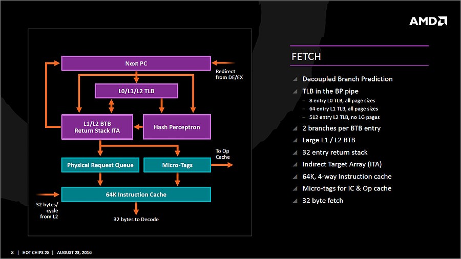
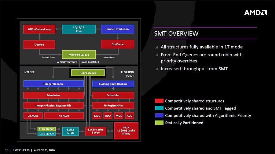
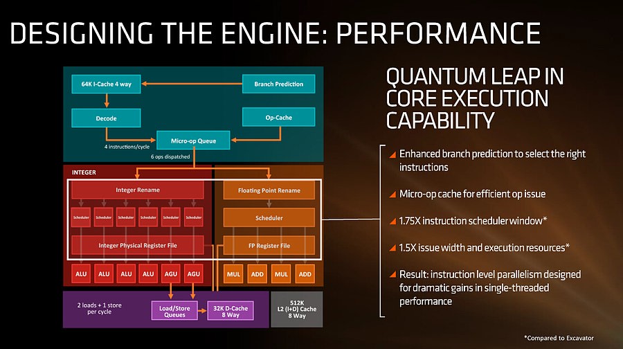
The cores themselves feature two threads each. The core complex hence comprises of 8 threads while the 8 core SKUs will comprise of 16 threads. On each core, branch misdirect is improved and the branch prediction has been improved with two branches per BTB. The large Op cache helps improve throughput and latency at the same time. The integer cluster in each Zen core has six pipes, four ALUs, Arithmetic Logic Units, and two AGUs which is short for Address Generation Units.
【每个核心有2个线程。1个CCX为8线程,8核版本就有2个CCX,16线程。分支目标缓冲(branch target buffer,BTB)中每项变为两个分支,因此分支预测也大大改善。大容量微指令缓存能同时提升吞吐量和延迟。整数簇有6条管线,4个ALU,2个AGU。】
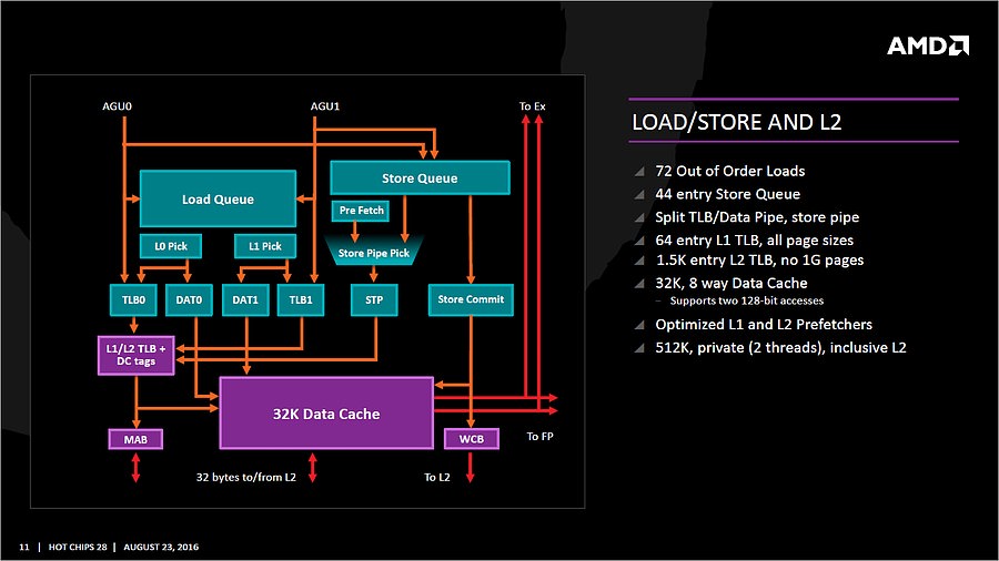
These AGUs can perform two 16-byte loads and one 16-byte store per cycle via a 32 KB 8-way set associative write-back L1 data cache. According to AMD the move from a write-through to a write-back cache has noticeably reduced stalls in several types of code paths. The load/store cache operations cache in Zen also reportedly exhibit lower latency compared to Excavator.
【AGU每周可以进行2次16byte的load操作和1次16byte的store操作(通过32KB 8路组相连回写式L1数据缓存)。前文也有提到,从穿透式改为回写式可以显著减少特定情况下的闲置时间。Zen上的L/S缓存操作缓存的延迟也比Excavator更低。】
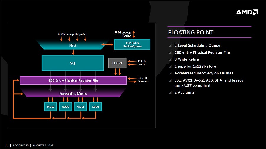
AMD has tried to improve Zen with a larger dispatch of 6 vs 4 on Excavator. Instruction schedulers for integer and floating point have also increased to 84 and 96, respectively. The FPU is now an Quad Issue while queue sizes for retire, load and store have increased to 192, 72, 44 compared to 128, 44, 32 on Excavator.
【Zen上的分发器为6条指令,比Excavator上的4条更大。整数和浮点单元的指令调度器也从84增加到了96.浮点单元现在是4发射了,退出、L/S操作的队列大小增加到了192、72、44,Excavator上为128、44、32。】
The two floating point units on the new core consist of 4 pipes with 128 FMACs per FPU. There are two FADD and two FMUL units for calculations on the FPU. The FPU consists of a 2-level scheduling queue with a 160 entry register file, 8-Wide retire and a single pipe for 128b store.It has its own two AES units and is SSE, AVX1, AVX2, AES, SHA and legacy MMX compliant.
【两个浮点单元依然是4条管线,每个单元128bit FMAC。有两个计算用的FADD和两个FMUL单元。浮点单元继续使用2级调度队列,它的寄存器为160项,退出宽度为8,还有一条供128b store操作的管线。此外还有两个AES加密单元,兼容SSE,AVX1,AVX2,AES,SHA和MMX指令集。】
AMD Zen With SMT (Simultaneous Multi-Threading Support)
【Zen的同步多线程】
One of the most anticipated arrival on the new core is SMT support. This brings the design level much closer to Intel’s implementation. The SMT design offers increased throughput by executing two threads simultaneously. These virtual threads will appear as independent cores to software and allow more execution resources at the hand applications.
【很多人早就预料到了Zen对同步多线程的支持。这使得Zen在设计层面上更加接近Intel。SMT设计能够通过同时执行两个线程来增加吞吐量,而且这两个线程在软件中都显示为独立核心。】
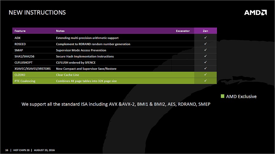
Along with the SMT support, Zen also features support for several new instructions. These include ADX, RDSEED, SMAP, SHA1, XSAVEC, CLZERO and PTE Coalescing. AMD also supports all the standard ISA that are mentioned above.
【随着SMT的支持,Zen也增加了新指令。包括ADX,RDSEED,SMAP,SHA1,XSAVEC,CLZERO和PTE Coalescing。当然AMD也会支持上面提到的所有标准指令集。】
AMD Zen High Bandwidth, Low Latency Cache System
【Zen的高带宽,低延迟缓存系统】
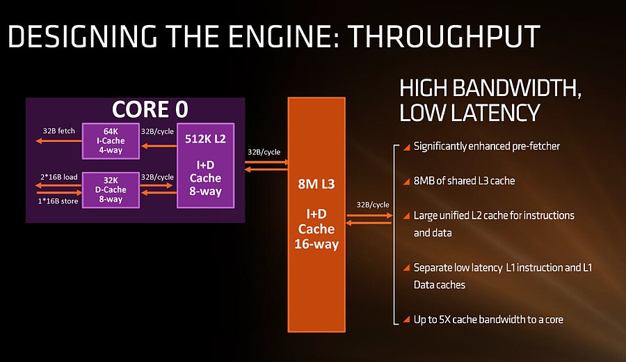
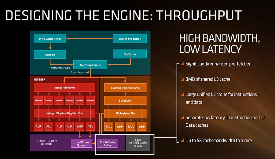
AMD has been talking about a disruptive cache system on their new core for a while. With the details finally out, we can now better understand this system. The cache hierarchy is made up of a fast private L2 cache on each core (512 KB L2 L+D 8-Way) and a fast shared L3 cache (8 MB L3 L+D 16-Way).
【AMD一直都在谈论新核心上革新的缓存系统。这次细节终于透露出来了,缓存架构由每核心上的高速独立L2(512KB L+D 8路关联)和高速共享L3(8MB L+D 16路关联)组成。】
This enables faster band width for prefetch improvements allowing faster cache-to-cache transfers. The L3 cache is mostly filled up of the L2 victims while offering larger queues for L1 and L2 misses.
【这带来了缓存之间很高的带宽,使得预取性能提升。L3缓存主要被L2的victim占据,同时给L1和L2未命中带来更大的队列。】
【注:victim的含义:Eviction驱逐
从cache移出一个line从而为新的数据腾出空间的过程我们成为Eviction。Eviction可以由用户发出的writeback-invalidate产生,被驱逐的line我们称为victim line。当victim line是dirty(“脏”)的时候,数据必须回写到下一级存储器中以维持内存的一致性。—来源:http://blog.csdn.net/shanghaiqianlun/article/details/6945497】
Each core also comprises of an 64K L1 L (4-Way) cache and 32K L1 D (8-Way) cache. The entire systems adds up to faster L1, L2 and L3 caches that offer faster load to FPU (7 cycles required). Bandwidth is improved to almost 2x on L1 and L2 while L3 cache system bandwidth is improved by 5x.
【每个核心还有64K L1 (4路关联)指令缓存和32KB L1 数据(8路关联)缓存。整个系统中更快的L1,L2,L3缓存能够使得FPU的load操作更快(需要7周期)。L1和L2带宽为原来的2倍,而L3带宽为5倍。】
AMD Zen ? A 14nm FinFET, Low Power and Faster Design
【Zen – 14nmFinFET的 低功耗高性能设计】
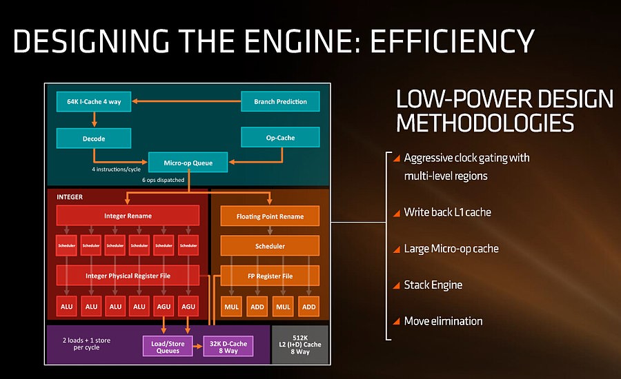
Performance is one thing but one place where AMD has really lacked is efficiency. With Zen, that is going to change. Zen has much higher efficiency than Excavator which is a highly tuned design in itself. This is achieved through the use of aggressive clock-gating techniques on multi-level regions inside the core block. Some of the features that help achieve lower power on Zen include:
【性能虽很重要,但AMD之前真正缺少的是能效。Zen上这种情况将会改变。Zen的能效比Excavator要高得多,而Excavator本身已经是高度优化过的架构。因为Zen上使用了激进的多层次多区块时钟门控技术。】
AMD Zen Low Power Features:
【Zen的低功耗特性】
- Aggressive Clock Gating with multi-level regions【激进的多层次多区块时钟门控】
- Write Back L1 Cache【写回式L1缓存】
- Large OP Cache【大容量微指令缓存】
- Stack Engine【堆栈引擎】
- Move Elimination【抱歉这个我不会翻译..】
- Power Focus from Project Inception【从计划开始阶段就看重功耗】
- Low Power design Methodologies【低功耗设计理念】

翻着玩 还好了
你挺幸苦的