【AMD Zen微架构解析 Part2:提取指令级并行】AMD Zen Microarchiture Part 2: Extracting Instruction-Level Parallelism
source:http://www.anandtech.com/show/10591/amd-zen-microarchiture-part-2-extracting-instructionlevel-parallelism
MD昨天半夜刚翻完WCCF的:http://www.moepc.net/?post=397
今天anandtech就出了part2….
心累 可能会大致翻一下
这TMD已经是第三篇了….
这篇比WCCF的要深入一些。
part1在这里:AMD Zen 微架构完全解析:双调度器,微指令缓存以及缓存架构

Hot Chips is an annual conference that allows semiconductor companies to present their latest and greatest ideas or forthcoming products in an academic-style environment, and is predominantly aimed as the professional semiconductor engineer. This year has a number of talks about power management, upcoming IBM CPUs, upcoming Intel CPUs, upcoming NVIDIA SoCs and the final talk of the final day is from AMD, discussing Zen in even more depth than the previous week. While we were unable to attend the event in person, we managed to get some hands on time with information and put questions to Mike Clark, AMD Senior Fellow and design engineer.
What We Learned Last Week: L1/L2/L3 Caches and the Micro-Op Buffer
【part1有讲的L1/L2/L3以及微指令缓存,可以翻上面的链接】
In AMD’s initial presentation for the general media, we were given a sense of the microarchitecture layout. We covered the material, but it contained a number of highlights.
AMD Zen Microarchitecture: Dual Schedulers, Micro-op Cache and Memory Hierarchy Revealed
AMD Server CPUs and Motherboard Analysis
Unpacking AMD’s Zen Benchmark: Is Zen actually 2% Faster than Broadwell?
First up, and the most important, was the announcement of the inclusion of a micro-op cache. This allows for instructions that are frequently used to be closer to the micro-op queue and saves a trip through the core and caches to load the desired information. Typically micro-op caches are still relatively small, and while AMD isn’t giving any information for size and accessibility, we know that Intel’s version can support 1536 uOps with 8-way associativity; we expect AMD’s to be similar though there are many options in play.
【首先也是最重要的是引入了微指令缓存,微指令缓存相对较小,现在数据未知,Intel的为1536条微指令,8路相连,AMD的应该也差不多】
Secondly is the cache structure. We were given details for the L1, L2 and L3 cache sizes, along with associativity, to compare it to former microarchitectures as well as Intel’s offering.
【Zen、推土机、挖掘机、SKL、BDW-E缓存对比】

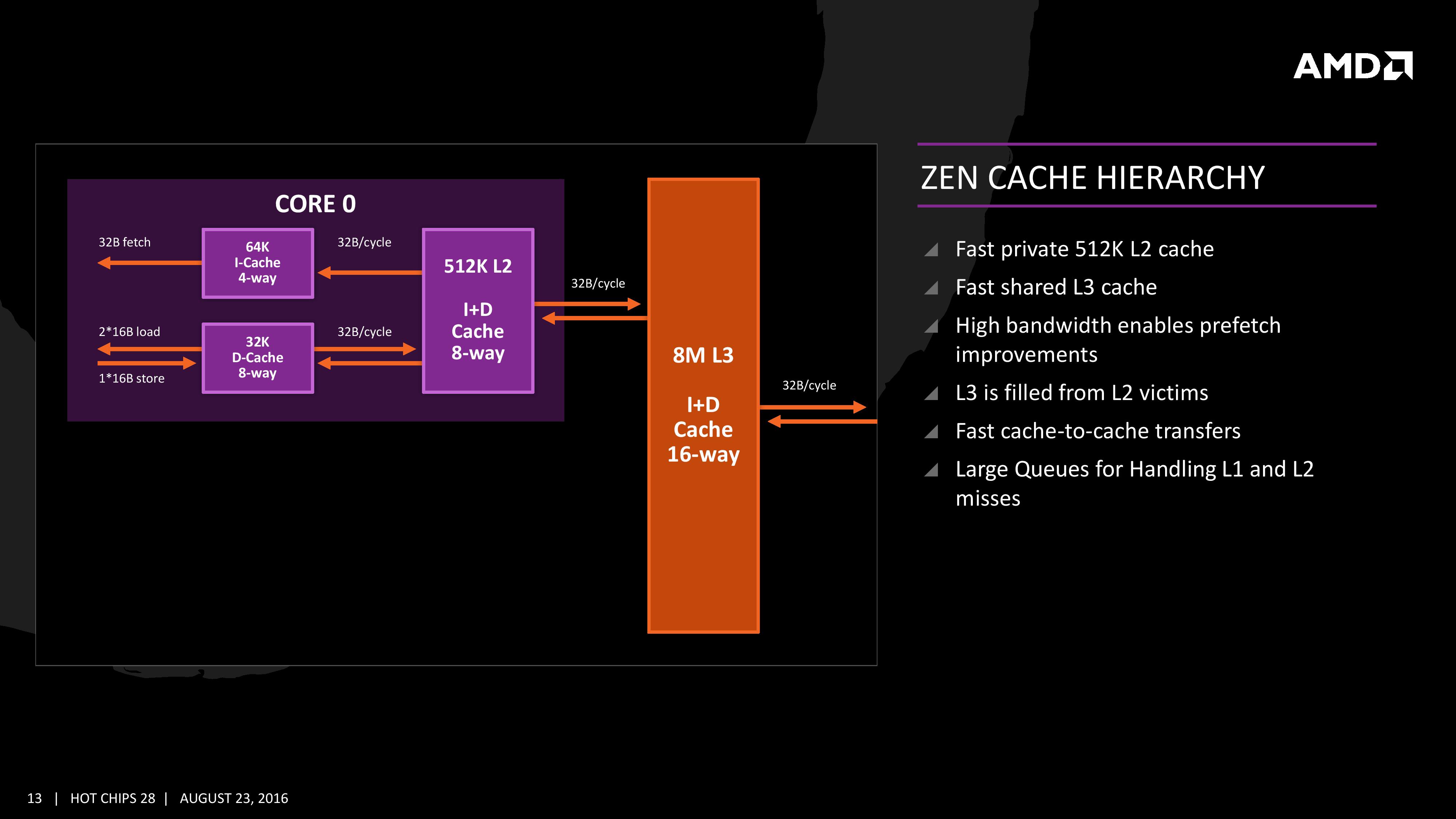
In this case, AMD has given Zen a 64KB L1 Instruction cache per core with 4-way associativity, with a lop-sided 32KB L1 Data cache per core with 8-way associativity. The size and accessibility determines how frequently a cache line is missed, and it is typically a trade-off for die area and power (larger caches require more die area, more associativity usually costs power). The instruction cache, per cycle, can afford a 32byte fetch while the data cache allows for 2x 16-byte loads and one 16-byte store per cycle. AMD stated that allowing two D-cache loads per cycle is more representative of the most workloads that end up with more loads than stores.
【L1数据指令缓存,详细介绍见前文】
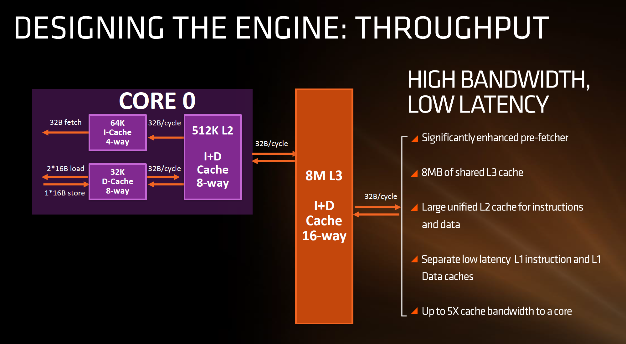
The L2 is a large 512 KB, 8-way cache per core. This is double the size of Intel’s 256 KB 4-way cache in Skylake or 256 KB 8-way cache in Broadwell. Typically doubling the cache size affords a 1.414 (square root of 2) better chance of a cache hit, reducing the need to go further out to find data, but comes at the expense of die area. This will have a big impact on a lot of performance metrics, and AMD is promoting faster cache-to-cache transfers than previous generations. Both the L1 and L2 caches are write-back caches, improving over the L1 write-through cache in Bulldozer.
【Zen的L2比SKL大一倍,命中率要高41.4%(2的平方根),但代价是更大的核心面积。】
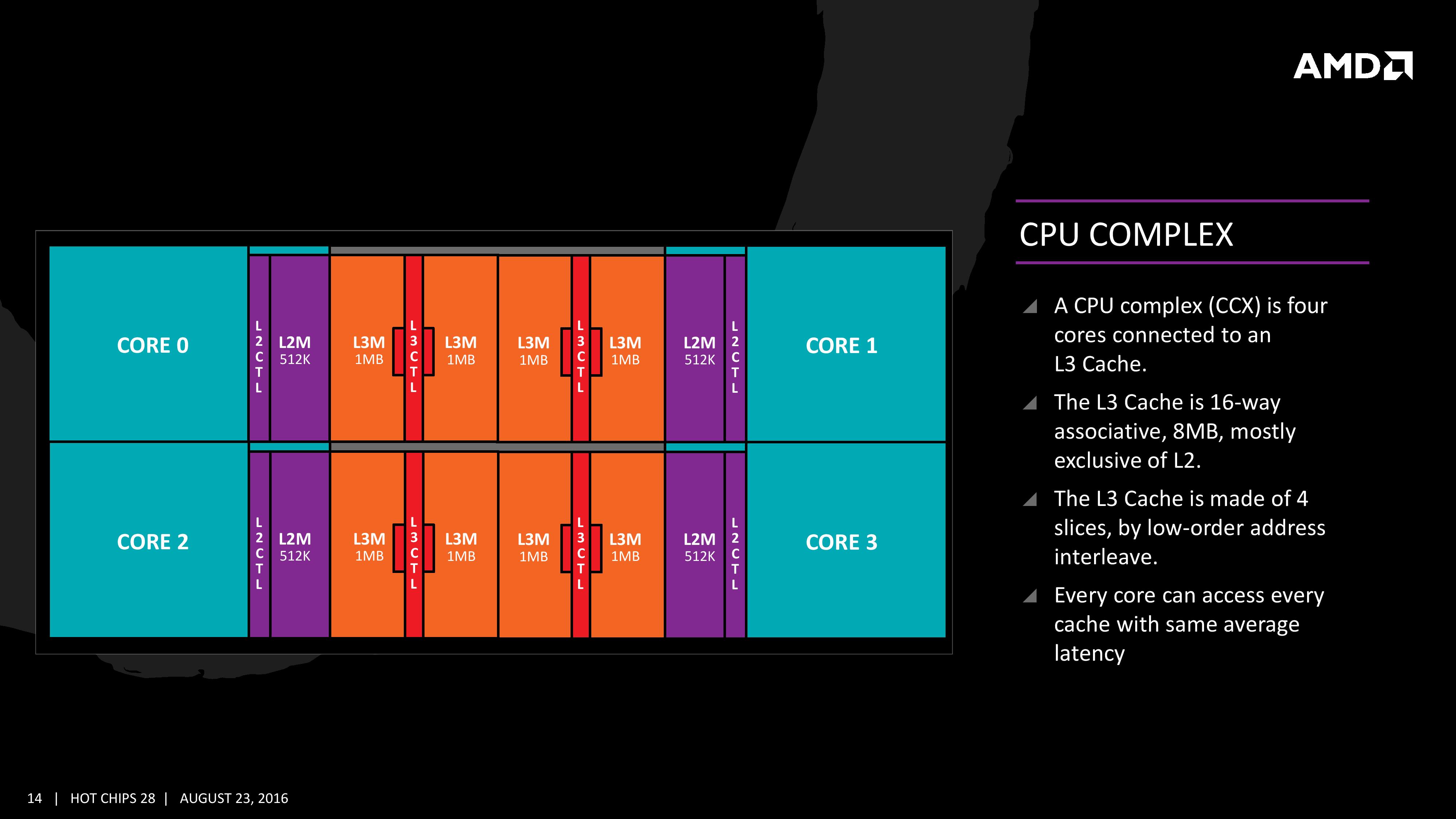
The L3 cache is an 8MB 16-way cache, although at the time last week it was not specified over how many cores this was. From the data release today, we can confirm rumors that this 8 MB cache is split over a four-core module, affording 2 MB of L3 cache per core or 16 MB of L3 cache for the whole 8-core Zen CPU. These two 8 MB caches are separate, so act as a last-level cache per 4-core module with the appropriate hooks into the other L3 to determine if data is needed. As part of the talk today we also learned that the L3 is a pure victim cache for L1/L2 victims, rather than a cache for prefetch/demand data, which tempers the expectations a little but the large L2 will make up for this. We’ll discuss it as part of today’s announcement.
The mid-week release also gave insight into the dual schedulers, one for INT and another for FP, which is different to Intel’s joint scheduler/buffer implementation. The talk at Hot Chips goes into detail about how the dispatch and schedulers operate
The New Information【新的信息】
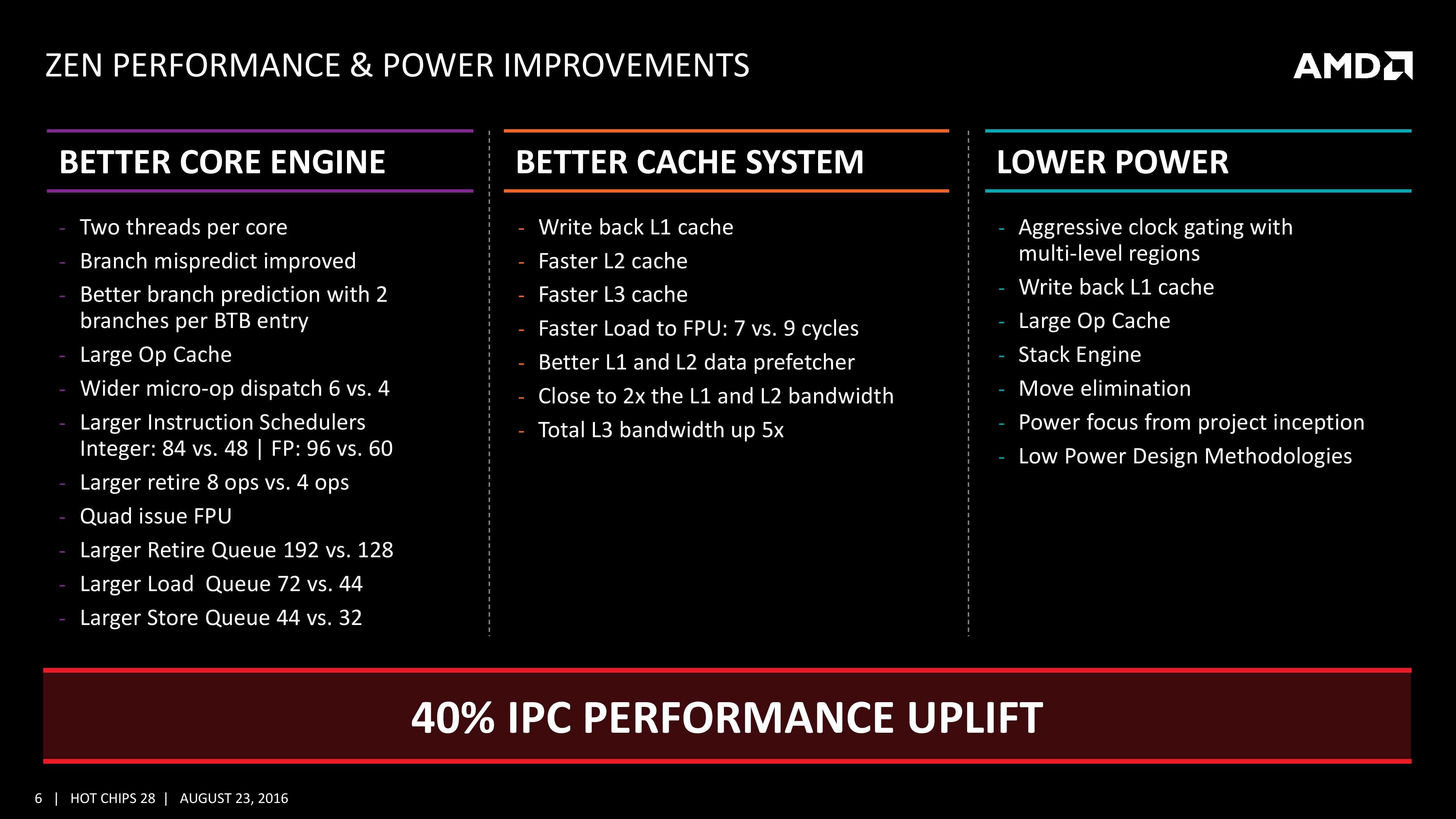
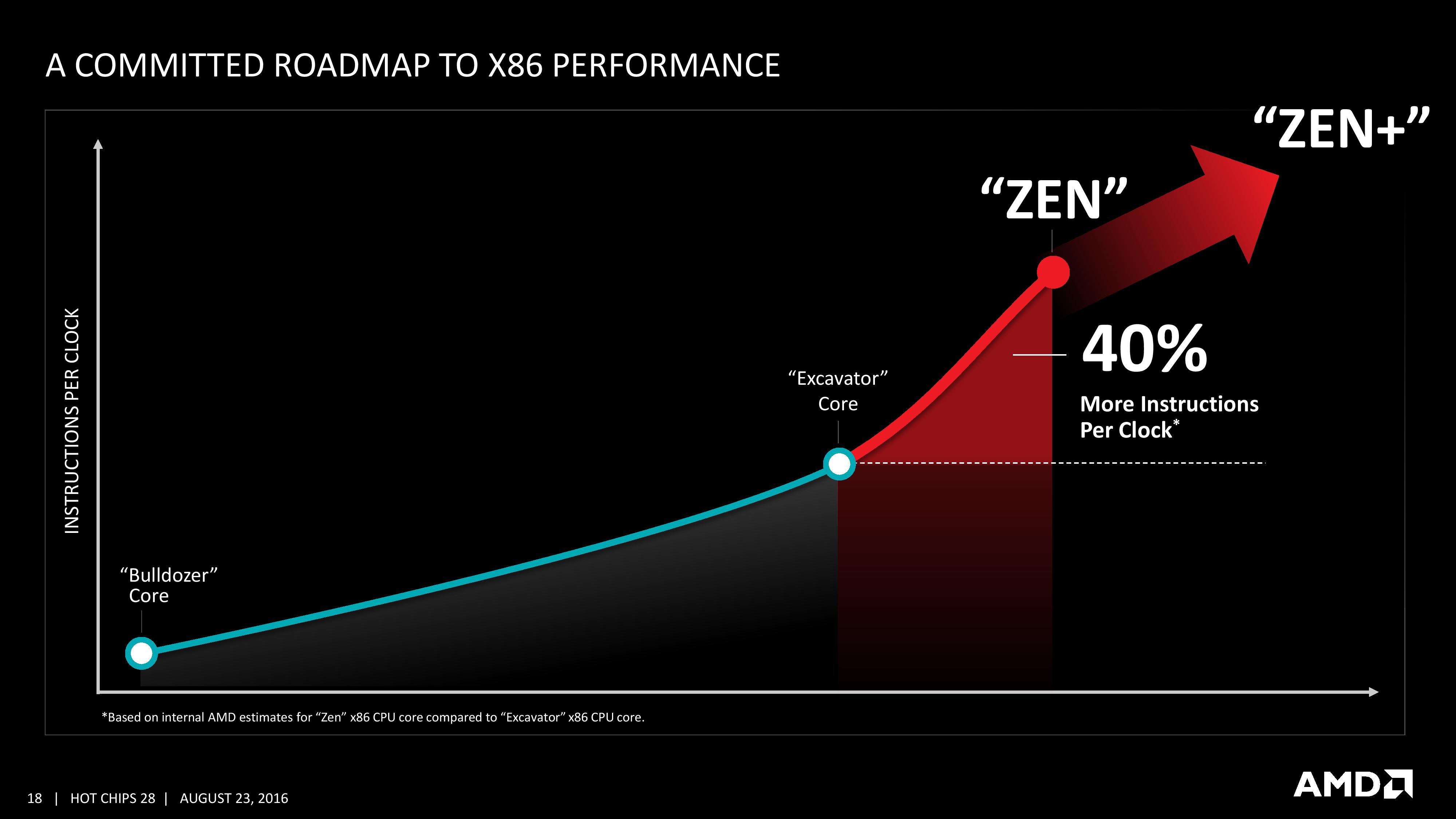
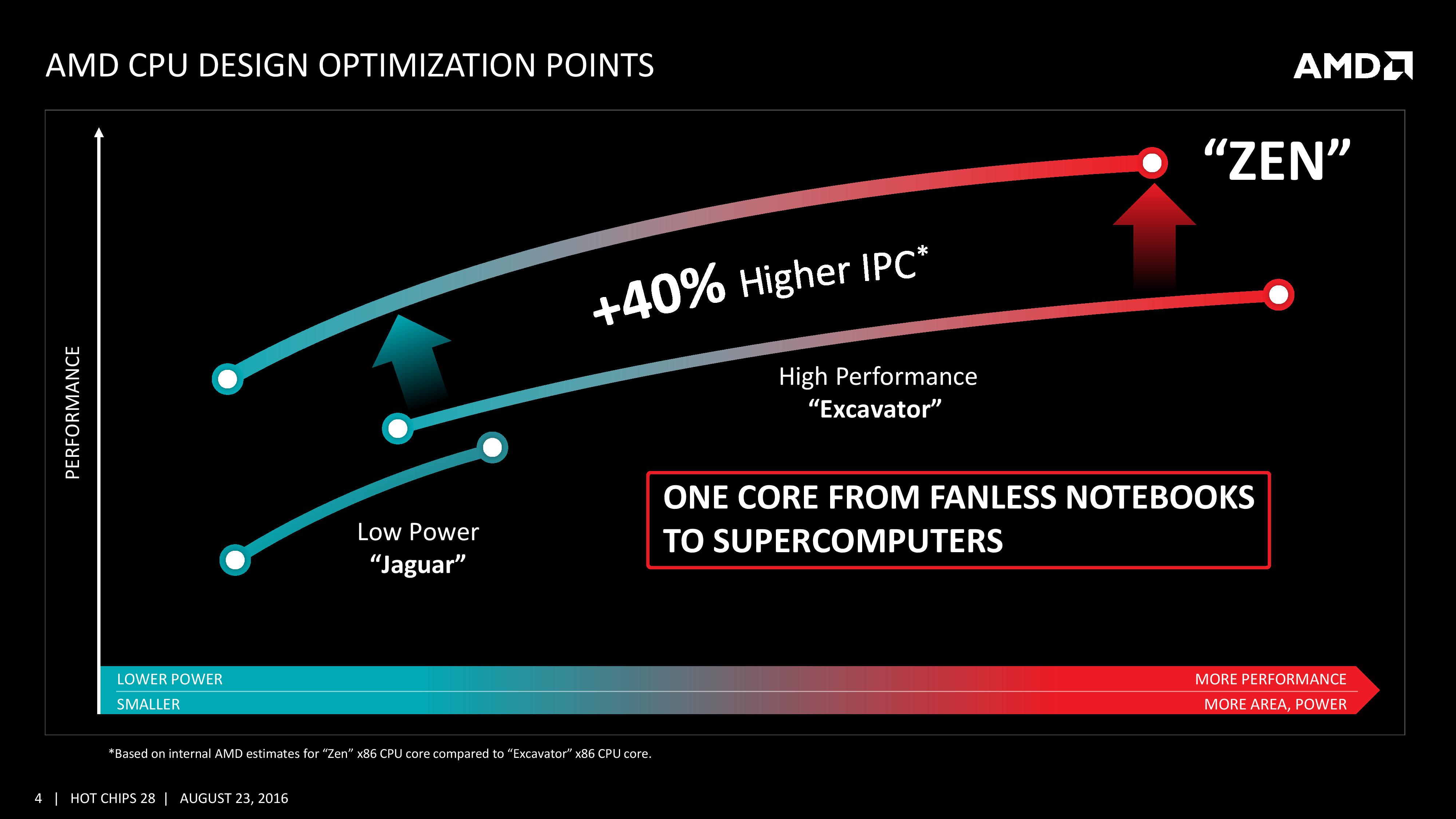
As part of the Hot Chips presentation, AMD is reaffirming its commitment to at least +40% IPC improvement over Excavator. This has specifically been listed as a throughput goal at an equivalent energy per cycle, resulting in an increase in efficiency. Obviously a number of benefits come from moving the 28nm TSMC process to GloFo’s 14nm FinFET process which is used via a Samsung licence. Both the smaller node and FinFET improvements have been well documented so we won’t go over them here, but AMD is stating that Zen is much more than this as a direct improvement to immediate performance, not just efficiency. While Zen is initially a high-performance x86 core at heart, it is designed to scale all the way from notebooks to supercomputers, or from where the Cat cores (such as Jaguar and Puma) were all the way up to the old Opterons and beyond, all with at least +40% IPC.

The first immediate image out of the presentation is the CPU Complex (a CCX), which shows the Zen core design as a four-CPU cluster with caches. This shows the L2/L3 cache breakdown, and also confirms 2MB of L3 per core with 8 MB of L3 per CCX. It also states that the L3 is mostly inclusive of the L2 cache, which stems from the L3 cache as a victim cache for L2 data. AMD is stating that the protocols involved in the L3 cache design allow each core to access the L3 of each other core with an average (but a range) of latencies.
【CCX单元,介绍可以在昨天翻译的WCCF文章里找到】
Over the next few pages, we’ll go through the slides. They detail more information about the application of Simultaneous Multithreading (SMT), New Instructions, the size of various queues and buffers, the back-end of the design, the front-end of the design, fetch, decode, execute, load/store and retire segments.
The High-Level Zen Overview【概观】
AMD is keen to stress that the Zen project had three main goals: core, cache and power. The power aspect of the design is one that was very aggressive ? not in the sense of aiming for a mobile-first design, but efficiency at the higher performance levels was key in order to be competitive again. It is worth noting that AMD did not mention ‘die size’ in any of the three main goals, which is usually a requirement as well. Arguably you can make a massive core design to run at high performance and low latency, but it comes at the expense of die size which makes the cost of such a design from a product standpoint less economical (if AMD had to rely on 500mm2 die designs in consumer at 14nm, they would be priced way too high). Nevertheless, power was the main concern rather than pure performance or function, which have been typical AMD targets in the past. The shifting of the goal posts was part of the process to creating Zen.
【AMD强调了Zen项目的三个主要目标:核心设计、缓存和功耗,其中功耗层面上会非常激进(不是挖掘机上专为移动版的设计,而是高性能下的高效设计)。】
This slide contains a number of features we will hit on later in this piece but covers a number of main topics which come under those main three goals of core, cache and power.
For the core, having bigger and wider everything was to be expected, however maintaining a low latency can be difficult. Features such as the micro-op cache help most instruction streams improve in performance and bypass parts of potentially long-cycle repetitive operations, but also the larger dispatch, larger retire, larger schedulers and better branch prediction means that higher throughput can be maintained longer and in the fastest order possible. Add in dual threads and the applicability of keeping the functional units occupied with full queues also improves multi-threaded performance.
For the caches, having a faster prefetch and better algorithms ensures the data is ready when each of the caches when a thread needs it. Aiming for faster caches was AMD’s target, and while they are not disclosing latencies or bandwidth at this time, we are being told that L1/L2 bandwidth is doubled with L3 up to 5x.
For the power, AMD has taken what it learned with Carrizo and moved it forward. This involves more aggressive monitoring of critical paths around the core, and better control of the frequency and power in various regions of the silicon. Zen will have more clock regions (it seems various parts of the back-end and front-end can be gated as needed) with features that help improve power efficiency, such as the micro-op cache, the Stack Engine (dedicated low power address manipulation unit) and Move elimination (low-power method for register adjustment – pointers to registers are adjusted rather than going through the high-power scheduler).
【L3以及低功耗设计,这部分也能在昨天翻译的文章中找到。】
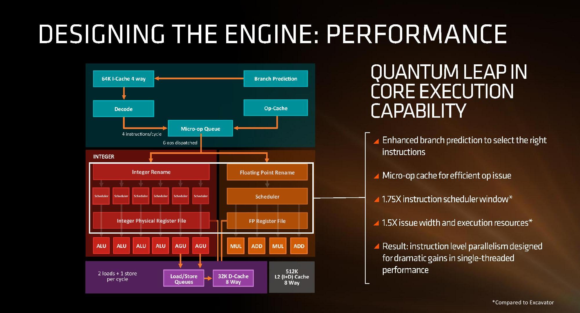
The Big Core Diagram
【核心设计】
We saw this diagram last week, but now we get updates on some of the bigger features AMD wants to promote:
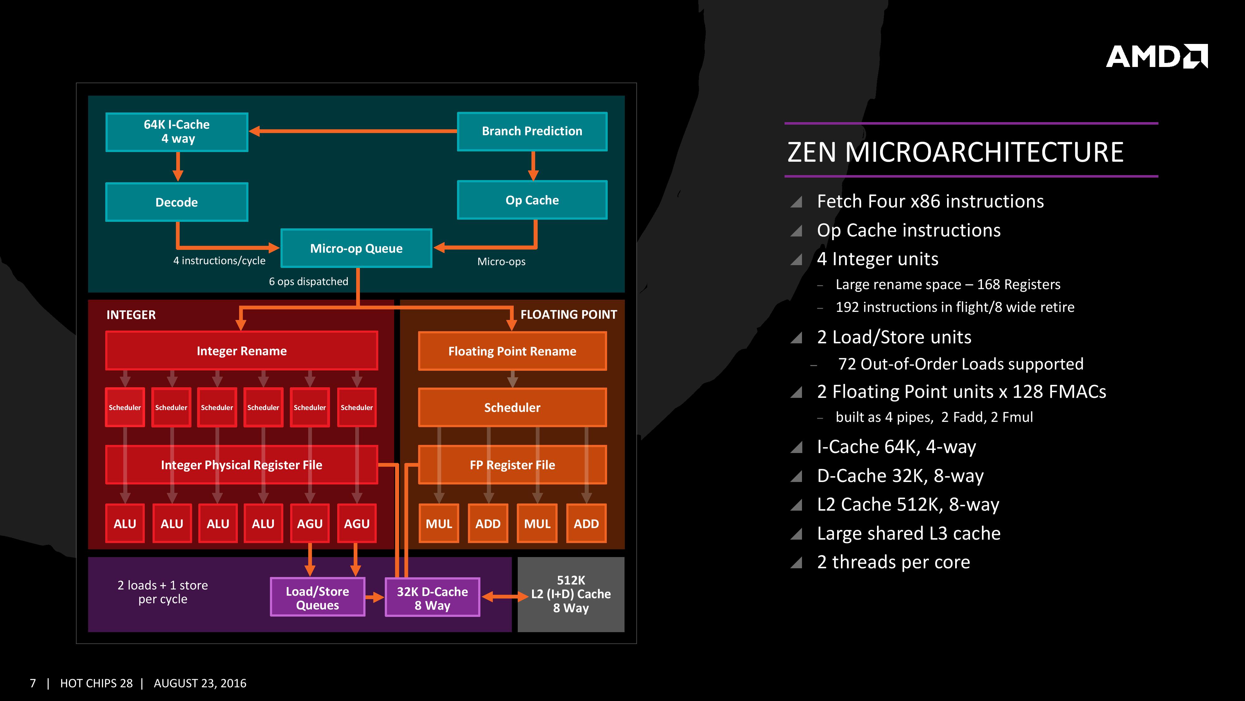
The improved branch predictor allows for 2 branches per Branch Target Buffer (BTB), but in the event of tagged instructions will filter through the micro-op cache. On the other side, the decoder can dispatch 4 instructions per cycle however some of those instructions can be fused into the micro-op queue. Fused instructions still come out of the queue as two micro-ops, but take up less buffer space as a result.
【分支预测的改进,解码器为4分发(在1条指令分发后拆分为2条微指令的情况下为6分发)】
As mentioned earlier, the INT and FP pipes and schedulers are separated, but the INT rename space is 168 registers wide, which feeds into 6×14 scheduling queues. The FP employs as 160 entry register file, and both the FP and INT sections feed into a 192-entry retire queue. The retire queue can operate at 8 instructions per cycle, moving up from 4/cycle in previous AMD microarchitectures.
【分离的整数/浮点调度器,整数 rename宽度为168,供6×14的调度队列使用。浮点寄存器为160项,整数和浮点公用192项的退出队列。退出队列每周期退出8条指令,相对前代翻倍】
The load/store units are improved, supporting a 72 out-of-order loads, similar to Skylake. We’ll discuss this a bit later. On the FP side there are four pipes (compared to three in previous designs) which support combined 128-bit FMAC instructions. These cannot be combined for one 256-bit AVX2, but can be scheduled for AVX2 over two instructions.
【LS单元支持和SKL相近。FP有4条管线,支持128bit FMAC指令,但不能合为1条256bit AVX2】
Fetch【取指】
For Zen, AMD has implemented a decoupled branch predictor. This allows support to speculate on incoming instruction pointers to fill a queue, as well as look for direct and indirect targets. The branch target buffer (BTB) for Zen is described as ‘large’ but with no numbers as of yet, however there is an L1/L2 hierarchical arrangement for the BTB. For comparison, Bulldozer afforded a 512-entry, 4-way L1 BTB with a single cycle latency, and a 5120 entry, 5-way L2 BTB with additional latency; AMD doesn’t state that Zen is larger, just that it is large and supports dual branches. The 32 entry return stack for indirect targets is also devoid of entry numbers at this point as well.
【分离的分支预测系统】
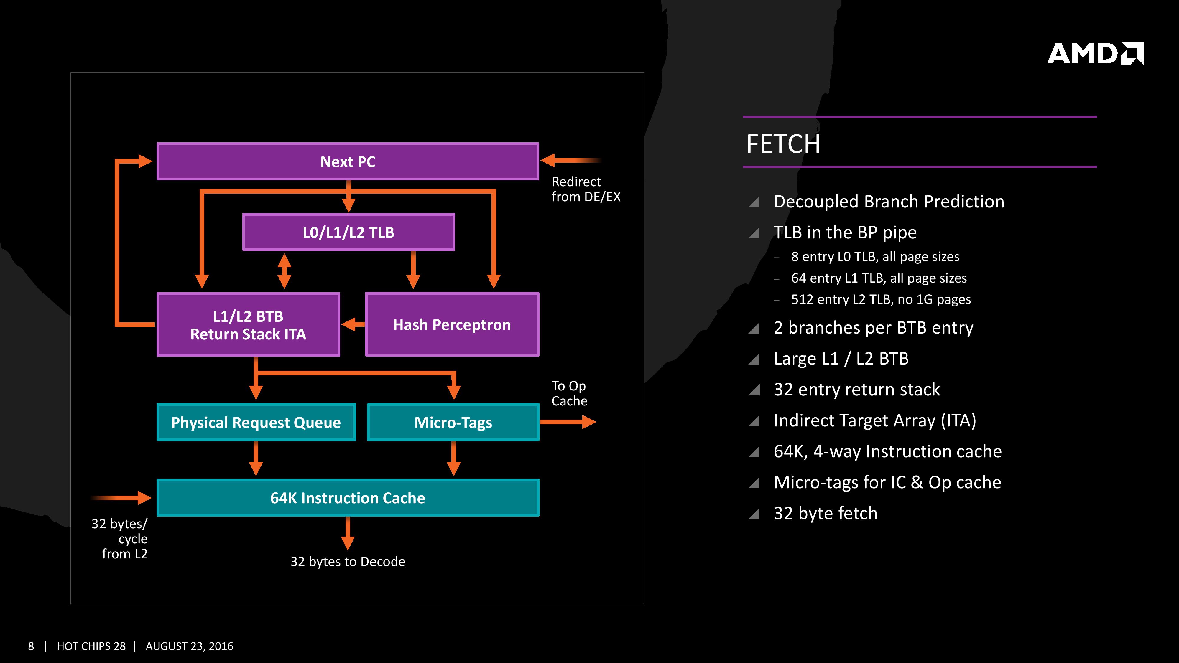
The decoupled branch predictor also allows it to run ahead of instruction fetches and fill the queues based on the internal algorithms. Going too far into a specific branch that fails will obviously incur a power penalty, but successes will help with latency and memory parallelism.
The Translation Lookaside Buffer (TLB) in the branch prediction looks for recent virtual memory translations of physical addresses to reduce load latency, and operates in three levels: L0 with 8 entries of any page size, L1 with 64 entries of any page size, and L2 with 512 entries and support for 4K and 256K pages only. The L2 won’t support 1G pages as the L1 can already support 64 of them, and implementing 1G support at the L2 level is a more complex addition (there may also be power/die area benefits).
【分支预测中TLB的改善:寻找最近使用过的转址来减少load延迟,在以下三个层级操作: L0 with 8 entries 任何页面大小, L1 with 64 entries 任何页面大小, 以及 L2 with 512 entries 只支持4K 和256K 页面。】
When the instruction comes through as a recently used one, it acquires a micro-tag and is set via the op-cache, otherwise it is placed into the instruction cache for decode. The L1-Instruction Cache can also accept 32 Bytes/cycle from the L2 cache as other instructions are placed through the load/store unit for another cycle around for execution.
Decode【解码】

The instruction cache will then send the data through the decoder, which can decode four instructions per cycle. As mentioned previously, the decoder can fuse operations together in a fast-path, such that a single micro-op will go through to the micro-op queue but still represent two instructions, but these will be split when hitting the schedulers. The purpose of this allows the system to fit more into the micro-op queue and afford a higher throughput when possible.
【每周期解码4指令,之前说过的单条指令拆分为2条微指令,能达到6条指令】
The new Stack Engine comes into play between the queue and the dispatch, allowing for a low-power address generation when it is already known from previous cycles. This allows the system to save power from going through the AGU and cycling back around to the caches.
【在队列和分发之间加入了新的堆栈引擎,能在低功耗下生成前几个周期使用过的地址,还能节省AGU和缓存周围传递数据的电能】
Finally, the dispatch can apply six instructions per cycle, at a maximum rate of 6/cycle to the INT scheduler or 4/cycle to the FP scheduler. We confirmed with AMD that the dispatch unit can simultaneously dispatch to both INT and FP inside the same cycle, which can maximize throughput (the alternative would be to alternate each cycle, which reduces efficiency). We are told that the operations used in Zen for the uOp cache are ‘pretty dense’, and equivalent to x86 operations in most cases.
【总的来说,这次做到了6分发,整数调度器为最高每周期6条,浮点调度器为每周期4条。这个调度单元可以同一周期内,同时向整数和浮点单元分发,最大化吞吐能力。】
Execution, Load/Store, INT and FP Scheduling【执行、L/S、整数和浮点调度】
The execution of micro-ops get filters into the Integer (INT) and Floating Point (FP) parts of the core, which each have different pipes and execution ports. First up is the Integer pipe which affords a 168-entry register file which forwards into four arithmetic logic units and two address generation units. This allows the core to schedule six micro-ops/cycle, and each execution port has its own 14-entry schedule queue.
【整数管线,168项寄存器,4ALU,2AGU,每周期调度6条指令,每个执行端口都有自己的14项调度队列。】
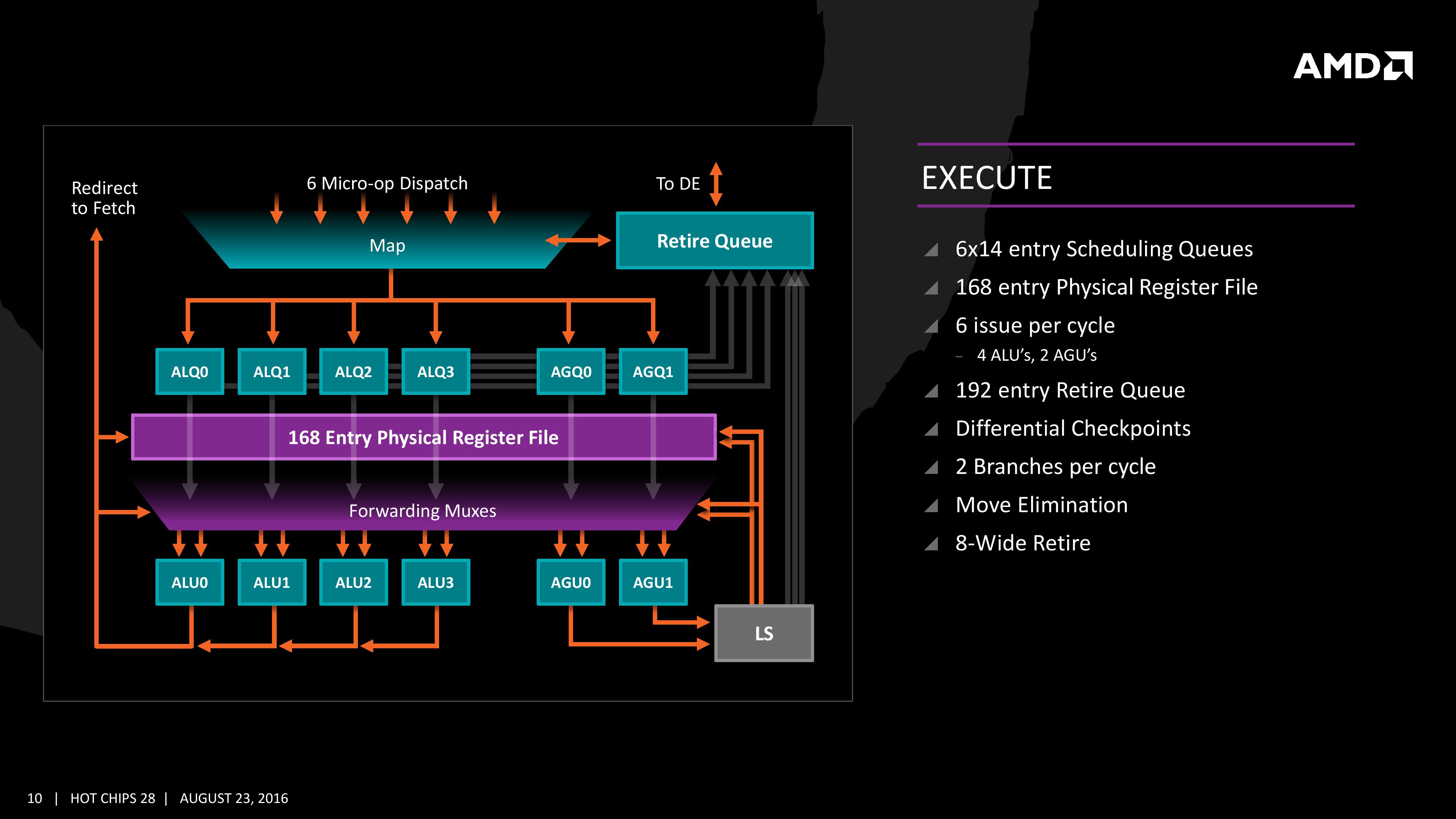
The INT unit can work on two branches per cycle, but it should be noted that not all the ALUs are equal. Only two ALUs are capable of branches, one of the ALUs can perform IMUL operations (signed multiply), and only one can do CRC operations. There are other limitations as well, but broadly we are told that the ALUs are symmetric except for a few focused operations. Exactly what operations will be disclosed closer to the launch date.
The INT pipe will keep track of branching instructions with differential checkpoints, to cut down on storing redundant data between branches (saves queue entries and power), but can also perform Move Elimination. This is where a simple mov command between two registers occurs ? instead of inflicting a high energy loop around the core to physically move the single instruction, the core adjusts the pointers to the registers instead and essentially applies a new mapping table, which is a lower power operation.
Both INT and FP units have direct access to the retire queue, which is 192-entry and can retire 8 instructions per cycle. In some previous x86 CPU designs, the retire unit was a limiting factor for extracting peak performance, and so having it retire quicker than dispatch should keep the queue relatively empty and not near the limit.
The Load/Store Units are accessible from both AGUs simultaneously, and will support 72 out-of-order loads. Overall, as mentioned before, the core can perform two 16B loads (2×128-bit) and one 16B store per cycle, with the latter relying on a 44-entry Store queue. The TLB buffer for the L2 cache for already decoded addresses is two level here, with the L1 TLB supporting 64-entry at all page sizes and the L2 TLB going for 1.5K-entry with no 1G pages. The TLB and data pipes are split in this design, which relies on tags to determine if the data is in the cache or to start the data prefetch earlier in the pipeline.

The data cache here also has direct access to the main L2 cache at 32 Bytes/cycle, with the 512 KB 8-way L2 cache being private to the core and inclusive. When data resides back in L1 it can be processed back to either the INT or the FP pipes as required.
Moving onto the floating point part of the core, and the first thing to notice is that there are two scheduling queues here. These are listed as ‘schedulable’ and ‘non-schedulable’ queues with lower power operation when certain micro-ops are in play, but also allows the backup queue to sort out parts of the dispatch in advance via the LDCVT. The register file is 160 entry, with direct FP to INT transfers as required, as well as supporting accelerated recovery on flushes (when data is written to a cache further back in the hierarchy to make room).
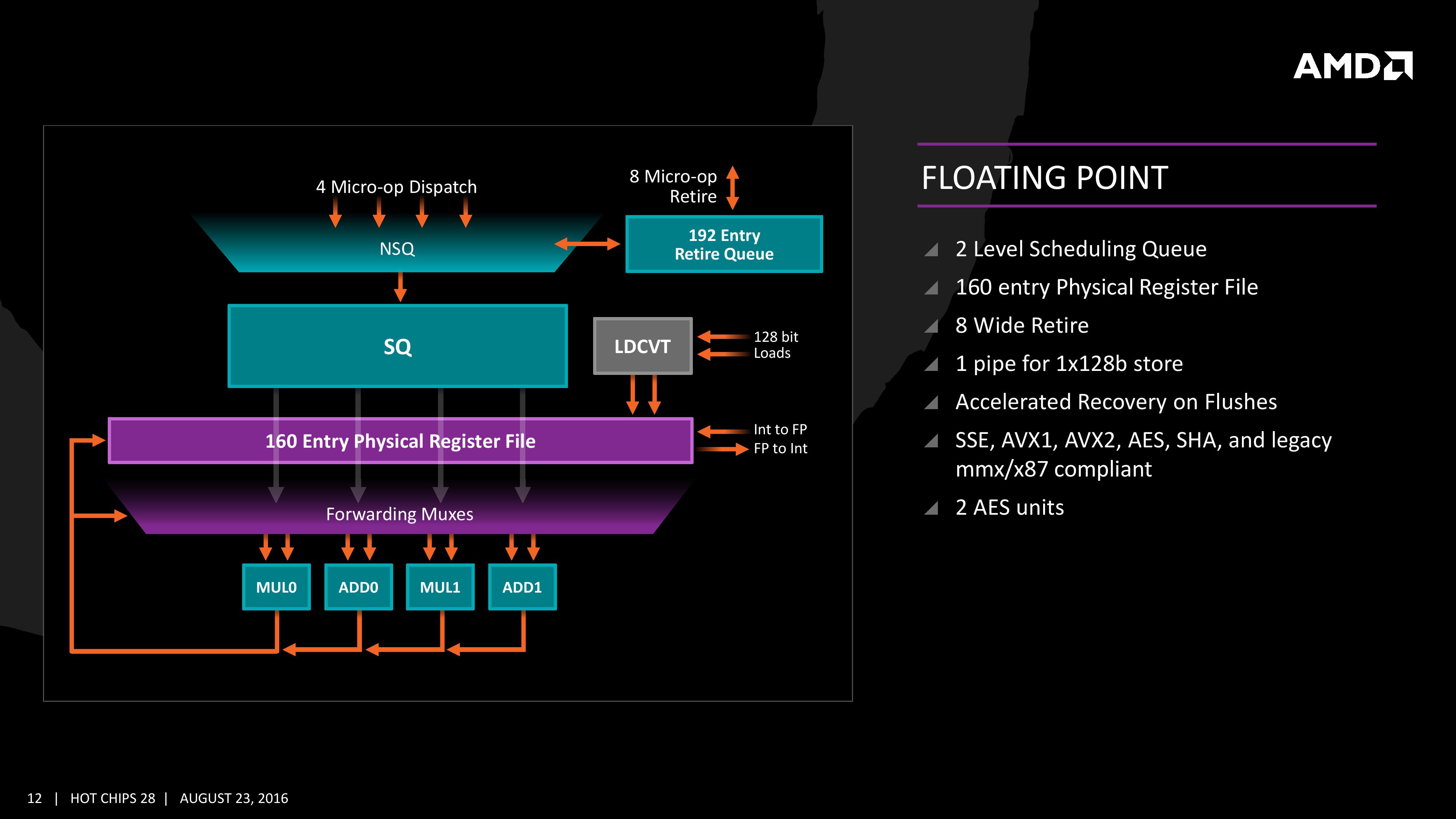
The FP Unit uses four pipes rather than three on Excavator, and we are told that the latency in Zen is reduced as well for operations (though more information on this will come at a later date). We have two MUL and two ADD in the FP unit, capable of joining to form two 128-bit FMACs, but not one 256-bit AVX. In order to do AVX, the unit will split the operations accordingly. On the counter side each core will have 2 AES units for cryptography as well as decode support for SSE, AVX1/2, SHA and legacy mmx/x87 compliant code.
The Core Complex, Caches, and Fabric【CCX结构、缓存】
Many core designs often start with an initial low-core-count building block that is repeated across a coherent fabric to generate a large number of cores and the large die. In this case, AMD is using a CPU Complex (CCX) as that building block which consists of four cores and the associated caches.
Each core will have direct access to its private L2 cache, and the 8 MB of L3 cache is, despite being split into blocks per core, accessible by every core on the CCX with ‘an average latency’ also L3 hits nearer to the core will have a lower latency due to the low-order address interleave method of address generation.
The L3 cache is actually a victim cache, taking data from L1 and L2 evictions rather than collecting data from prefetch/demand instructions. Victim caches tend to be less effective than inclusive caches, however Zen counters this by having a sufficiency large L2 to compensate. The use of a victim cache means that it does not have to hold L2 data inside, effectively increasing its potential capacity with less data redundancy.
It is worth noting that a single CCX has 8 MB of cache, and as a result the 8-core Zen being displayed by AMD at the current events involves two CPU Complexes. This affords a total of 16 MB of L3 cache, albeit in two distinct parts. This means that the true LLC for the entire chip is actually DRAM, although AMD states that the two CCXes can communicate with each other through the custom fabric which connects both the complexes, the memory controller, the IO, the PCIe lanes etc.
One interesting story is going to be how AMD’s coherent fabric works. For those that follow mobile phone SoCs, we know fabrics and interconnects such as CCI-400 or the CCN family are optimized to take advantage of core clusters along with the rest of the chip. A number of people have speculated that the fabric used in AMD’s new design is based on HyperTransport, however AMD has confirmed that they are not using HyperTransport here for Zen. More information on the fabric may come out as we nearer the launch, although this remains one of the more mysterious elements to the design at this stage.

The cache representation in the new presentation at Hot Chips is almost identical to that in midweek, showing L1 and L2 in the core with 8MB of L3 split over several cores. AMD states that the L1 and L2 bandwidth is nearly double that of Excavator, with L3 now up to 5x for bandwidth, and that this bandwidth will help drive the improvements made on the prefetch side. AMD also states that there are large queues in play for L1/L2 cache misses.
Simultaneous MultiThreading (SMT)【同步多线程】
Zen will be AMD’s first foray into a true simultaneous multithreading structure, and certain parts of the core will act differently depending on their implementation. There are many ways to manage threads, particularly to avoid stalls where one thread is blocking another that ends in the system hanging or crashing. The drivers that communicate with the OS also have to make sure they can distinguish between threads running on new cores or when a core is already occupied ? to achieve maximum throughput then four threads should be across two cores, but for efficiency where speed isn’t a factor, perhaps power gating/clock gating half the cores in a CCX is a good idea.

There are a number of ways that AMD will deal with thread management. The basic way is time slicing, and giving each thread an equal share of the pie. This is not always the best policy, especially when you have one performance dominant thread, or one thread that creates a lot of stalls, or a thread where latency is vital. In some methodologies the importance of a thread can be tagged or determined, and this is what we get here, though for some of the structures in the core it has to revert to a basic model.
With each thread, AMD performs internal analysis on the data stream for each to see which thread has algorithmic priority. This means that certain threads will require more resources, or that a branch miss needs to be prioritized to avoid long stall delays. The elements in blue (Branch Prediction, INT/FP Rename) operate on this methodology.
A thread can also be tagged with higher priority. This is important for latency sensitive operations, such as a touch-screen input or immediate user input elements required. The Translation Lookaside Buffers work in this way, to prioritize looking for recent virtual memory address translations. The Load Queue is similarly enabled this way, as typically low latency workloads require data as soon as possible, so the load queue is perfect for this.
Certain parts of the core are statically partitioned, giving each thread an equal timing. This is implemented mostly for anything that is typically processed in-order, such as anything coming out of the micro-op queue, the retire queue and the store queue.
The rest of the core is competitive, meaning that if a thread demands more resources it will try to get there first if there is space to do so each cycle.
New Instructions【新指令集】
AMD has a couple of tricks up its sleeve for Zen. Along with including the standard ISA, there are a few new custom instructions that are AMD only.
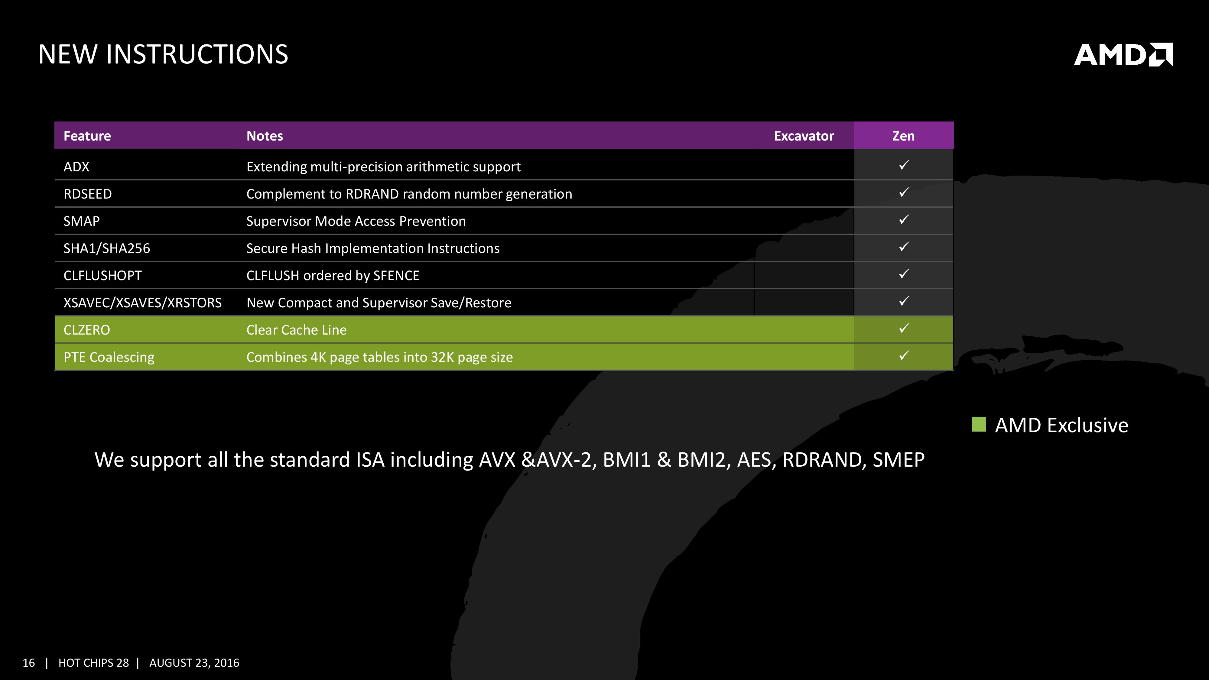
Some of the new commands are linked with ones that Intel already uses, such as RDSEED for random number generation, or SHA1/SHA256 for cryptography. The two new instructions are CLZERO and PTE Coalescing.
The first, CLZERO, is aimed to clear a cache line and is more aimed at the data center and HPC crowds. This allows a thread to clear a poisoned cache line atomically (in one cycle) in preparation for zero data structures. It also allows a level of repeatability when the cache line is filled with expected data. CLZERO support will be determined by a CPUID bit.
PTE (Page Table Entry) Coalescing is the ability to combine small 4K page tables into 32K page tables, and is a software transparent implementation. This is useful for reducing the number of entries in the TLBs and the queues, but requires certain criteria of the data to be used within the branch predictor to be met.
Some Final Thoughts and Comparisons【总结和对比】
With the Hot Chips presentation we’ve been given more information on the Zen core microarchitecture than we expected to have at this point in the Zen design/launch cycle. AMD has already stated that general availability for Zen will be in Q1, and Zen might not be the final product launch name/brand when it comes to market. However, there are still plenty of gaps in our knowledge for the hardware, and AMD has promised to reveal this information as we get closer to launch.
We discussed in our earlier piece on the Zen performance metrics given mid-week that it can be hard to interpret any anecdotal benchmark data at this point when there is so much we don’t know (or can’t confirm). With the data in this talk at Hot Chips, we can fill out a lot of information for a direct comparison chart to AMD’s last product and Intel’s current offerings.

Bulldozer uses AMD-coined macro-ops, or Mops, which are internal fixed length instructions and can account for 3 smaller ops. These AMD Mops are different to Intel’s ’macro-ops’, which are variable length and different to Intel’s ’micro-ops’, which are simpler and fixed-length.
Excavator has a number of improvements over Bulldozer, such as a larger L1-D cache and a 768-entry L1 BTB size, however we were never given a full run-down of the core in a similar fashion and no high-end desktop version of Excavator will be made.
This isn’t an exhaustive list of all features (thanks to CPU World, Real World Tech and WikiChip for filling in some blanks) by any means, and doesn’t paint the whole story. For example, on the power side of the equation, AMD is stating that it has the ability to clock gate parts of the core and CCX that are not required to save power, and the L3 runs on its own clock domain shared across the cores. Or the latency to run certain operations, which is critical for workflow if a MUL operation takes 3, 4 or 5 cycles to complete. We have been told that the FPU load is two cycles quicker, which is something. The latency in the caches is also going to feature heavily in performance, and all we are told at this point is that L2 and L3 are lower latency than previous designs.
A number of these features we’ve already seen on Intel x86 CPUs, such as move elimination to reduce power, or the micro-op cache. The micro-op cache is a piece of the puzzle we want to know more about, especially the rate at which we get cache hits for a given workload. Also, the use of new instructions will adjust a number of workloads that rely on them. Some users will lament the lack of true single-instruction AVX-2 support, however I suspect AMD would argue that the die area cost might be excessive at this time. That’s not to say AMD won’t support it in the future ? we were told quite clearly that there were a number of features originally listed internally for Zen which didn’t make it, either due to time constraints or a lack of transistors.
We are told that AMD has a clear internal roadmap for CPU microarchitecture design over the next few generations. As long as we don’t stay for so long on 14nm similar to what we did at 28/32nm, with IO updates over the coming years, a competitive clock-for-clock product (even to Broadwell) with good efficiency will be a welcome return.
找到了!可WCCF那篇没有这篇详细,建议你有时间重新翻译。这篇可是硬通货科技文,是A媒体的Zen架构重点介绍。强烈建议重新翻译,WCCF那篇可以删了,因为没有多少人看的。(WCCF假新闻太多,没有A专业)
http://www.moepc.net/?post=397
WCCF那篇链接在哪?
我之前已经发过两篇完整翻译
这一篇内容基本相同。
你傻啊!!!
这么详细的架构介绍文,给你翻译成这样?幸亏我九年前高中毕业,英语还可以!(当时高中英语难度,相当于英语四级)[嘻嘻]
哦,是吗
垃圾马文