原文作者:David Schor
原文地址:https://fuse.wikichip.org/news/641/iedm-2017-globalfoundries-7nm-process-cobalt-euv/
划重点下划线部分是我加的
IEDM 2017: GlobalFoundries 7nm process; Cobalt, EUV
We have known for a while now that GlobalFoundries was planning an aggressive shrink of their 14nm process. At the 63rd IEEE International Electron Devices Meeting (IEDM), GlobalFoundries presented their “late” paper on their 7nm process ? “7nm Leading Performance” or “7LP” for short. The paper was presented by Dr. Premlatha Jagannathan. Jagannathan is responsible for the advanced technology materials engineering at GlobalFoundries.
The focus of the paper was about their 7nm CMOS technology platform for mobile and high-performance computing applications. The paper presented the work that was done by their 7nm development team.
Overview
We will start off with the laundry list of features and then dive into the specifics. The general attributes of this process are:
Targets Mobile, SoC, HPC
2.8x routed logic density over their 14nm
Provides 40% higher performance or 55% lower power over their 14nm
Immersion lithography and advanced optical patterning (SADP, SAQP)
Cobalt introduced for liner and the caps at the SAQP-critical layers
EUV insertion plan in place, undefined timeline (i.e., “when ready”)
Backbone of their next-generation ASIC services
Complete set of foundation and complex IP available (e.g., core, peripherals, SerDes, Memories, 2 & 2.5D packaging)
14nm Reference Technology
Throughout the IEDM presentation, they made many comparisons against a 14nm reference node. This 14nm node was initially presented by Samsung at the 2014 IEEE International Solid-State Circuits Conference (ISSCC). Their 14nm node has been in production for over two years and has been used for a very diverse set of applications including high-performance computing, networks, and mobile application processors. A well-known example of such product is AMD’s Zen microarchitecture.
With that respect, their 7nm brings a full node density and performance scaling over the 14nm reference.
Key Dimensions
The key technology dimensions are shown below.

As expected, GlobalFoundries is continuing with the use of a FinFET transistor. Their 7nm process features an aggressive fin pitch of just 30 nm which means Self-Aligned Quadruple Patterning (SAQP) will be utilized here. The gate pitch is at 56 nm. The 1x metal layers have a pitch of 40nm and are unidirectional. Like the gate patterning, the 1x metal layers will also make use of just Self-Aligned Dual Patterning (SADP). Note that three of the four layers listed are at 1x (M0, M2, and M3). M1 has a relaxed pitch of 56nm which is aligned with the gate.
As a side note, GF listed this technology as their third generation FinFET however 14nm was their first generation FinFET so we’re not exactly sure what they consider their second generation. It’s possible they refer to their 12nm as 2nd generation. However if that’s the case, apparently they did not seem to think it was important enough to list it on the roadmap they presented at IEDM which only listed 20nm, 14nm, and their 7nm.
Going After the Density
The aggressive scaling of design rules allowed GlobalFoundries to significantly scale of the standard cell. In their 14nm process, GlobalFoundries’ workhorse cell was a 9-tracks, four fin cell.

WikiChip’s illustration of a 4-fin, 9T cell as used by GF for their 14nm process
Having a metal pitch of 64 nm, this cell had the height of 576 nm.
In their new 7nm process, the new workhorse cell is a 2-fin, 6-track cell. With a metal pitch of 40nm, the new cell has a cell height of just 240nm.

WikiChip’s illustration of a 2-fin, 6T cell as used by GF for their 7nm process
This very aggressive scaling which resulted in 0.42x in cell height reduction has an even larger impact at the SoC level. GlobalFoundries reports that the overall compaction compared to their 14nm reference is 0.36x at the SoC level (i.e., a mixture of various critical cells such as combinational gates, multi-input gates, complex cells, and flip-flops).

7nm cell performance vs frequency vs 14nm
The graph above compares the power vs. the frequency of their 14nm reference node to their 7nm node. What can be seen is that for the same given power, there is 40% gain in performance. Alternatively, you can think of it as having >55% power reduction at a fixed frequency.
Efficient Routing
In order to accomplish efficient scaling at the SoC level, it’s not enough to just scale the cell. GlobalFoundries had to rework and optimize their routing rules. Dr. Jagannathan listed a number of optimizations they have done in order to achieve the desired post-route scaling. Those include logic cell design by removing the various blockages, intelligent pin placement, and various routing optimizations. GF did not detail those optimizations any further for us to be able talk about them. All of those optimizations are part of their new ground rules.

Routability improvements by various design optimizations
The graph above plots design rule checks (DRC) against utilization of of various design optimization cases introduced where case 2 refers to the cell design optimization and case 3 for the pin optimization. Together, all three optimizations were necessary in order for their 7nm process to achieve the 2.8x routed logic density goal.
High-Performance Cells
The 2-fin cell isn’t suitable for all applications and for high-performance computing GlobalFoundries 7nm process also offers a 4-fin logic cell.

WikiChip’s illustration of a 4-fin, 9T cell as used by GF for their 7nm process for the HP cells.
This cell is a 9-track cell meaning the cell height is 360 nm. More fins alone is not enough and for those high-performance applications there is a need for larger power grids and large wires. For that, whereas the 2-fin 6T logic cells featured minimum Mx pitches for height scaling, the 4-fin 9T logic cell makes use of larger wire dimensions and increased contact sizes and vias. This was done in order to limit the IR drop and maximize performance. GlobalFoundries developed simultaneous support for a large range of wide wires and large contact and vias that make use of SADP for power grid, high-performance, and also custom high-speed analog and mix signal work.

Voltage swing and transition time benefit from wider wires and contacts
Wide wires and large contacts greatly benefits applications such as high-speed buffer designs or low RC intra-blocking wiring in large memories. The graph above illustrates the impact of a buffer designed for high-speed SerDes (HSS) application. The SPICE voltage trace shows a 30% improvement in the rise time when optimizing the design using wide wires and contacts.
The extra drive strength that is available through the extra fins allows them to scale to higher frequencies that are a necessity for high-performance applications.

7nm cell performance vs frequency vs 14nm for both their SoC (6T, 2-fin cells) and HPC (9T, 4-fin cells)
The graph above shows the performance extendibility achieved by the 4-fin logic cell. This is a very important requirement for high-end server applications that focus on single-thread performance (e.g., IBM’s z/Architecture and POWER).
Device Architecture
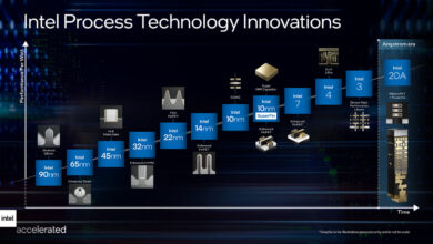
GlobalFoundries calls this architecture their 3rd generation FinFET. However, since GF only introduced FinFET in their last generation (14nm), we are not really sure what they consider 2nd generation. As we noted earlier, even during the presentation there was nothing in between their 14nm and their 7nm on their roadmap. Your guess would be as good as ours although we can’t help but imagine that at least some marketing is involved here (Keep in mind that Intel’s 10nm is a “true” 3rd generation FinFET, first introduced at their 22nm node, a full node ahead of everyone else).

The Fin is pitch is 30nm, meaning quad patterning is being employed here. We also measured a fin height of ~42nm which coincidentally happened to be the same height as Intel’s 14nm and their newly introduced 22FFL. The fin shape has been carefully optimized to improve the short-channel effects. The graph below clearly shows the improvement in DIBL vs the Leff when comparing the 7nm node to their 14nm process due to the fin profile optimizations that were done. For the same DIBL levels, there is a gain of roughly 4nm for the Leff.

This is also their 2nd generation of their (actually IBM’s) multi-workfunction (multi-WF) approach for device Vt. The multi-WF (in their 14nm they introduced dual-WF) process is used to generate widely-spaced Vts for both N/P without relying on doping to create the Vt separation. The underlying concept is undoped fins. Undoped fins introduce the benefits of higher mobility gains as well as it reduces the random dopant fluctuation (RDF)-induced threshold voltage (VT) variability (RDF-Vt mismatches). They first introduced this process with their 14nm SOI which had 4 undoped fins and 4 workfunction materials. In their 7nm this was enhanced to cover the entire range of Vts and this was enabled through the integration of eight additional workfunction materials.

Vt mismatch improvements
GlobalFoundries 7nm covers the entire Vt range from very low leakage devices to very high performance. In the graph above GlobalFoundries compared their 14nm undoped fins against their 7nm undoped fins. GF reported around 30% lower mismatch which was obtained with this process.

Id-Vg subthreshold swing
Shown is the reported subthreshold swing of ~70mV/dec and DIBL of ~40/50mV/V for N/P.

Additionally, GF introduced junction/epi and contact resistance optimizations in order to reduce the FinFET parasitic resistance. Those optimizations were required for them to reach the targeted effective current levels. The left graph shows the Idoff vs the Ieff which shows that vs the baseline, there is 15% improvement in the external resistance from the junction depth optimization doping. To improve the other components that affect the external resistance, GF optimized the interface between the contact and the epi. The graph on the right shows the Idoff vs the Ieff for the base case vs the contact resistance reduction optimizations. GlobalFoundries reported 30% improvement over the base case.
SRAM
As is usually the case when reporting on a new process, GlobalFoundries presented their SRAM bitcell offerings. Two cells were presented, a high-performance cell (PU:PG:PD = 1:2:2) and a high-density cell (PU:PG:PD = 1:1:1).

Note that the SRAM sizes for their 14nm came from their 2017 IEEE Symposium on VLSI Technology presentation. The 7nm SRAM was reported at this IEDM.

Densty & Array speed comparson
In the graph above GlobalFoundries compares the 14nm reference node to their 7nm in normalized density and array speed. What’s immediately obvious is just how well the two cell (1-1-1 and 1-2-2) scaled from the 14nm to the 7nm process. GF reported over 2.3x improvement in array density. Similarly, they also reported 2x in array speed performance. Jagannathan explained that the array speed improvement came from lower bit line capacitance and significant improvement in the read current. Note that the majority of the read current improvement came from the reduction in RDF-Vt mismatches which we talked about earlier.
Back-End
Two separate metallization stacks were designed for the 7nm process: a general-purpose stack and a high-performance stack. This allows flexibility in applications for anywhere from density to performance.
General-Purpose Stack
The general-purpose stack is 13 levels:

As a side note, their paper says the general-purpose stack has 13 interconnect layers but it really has 14 layers when we count M0. There is an advanced MIM cap available for the M13 layer used to decouple strong power supply.
High-Performance Stack
For the high-performance stack GlobalFoundries developed an 18-layer metallization stack. For this stack there was a need for very low resistance in the power grid and for that GF added optional layers available at 6.4x, 9x, and 60x. Note that the advanced MIMcap is available here at the 60x level.

40nm restriction, Cobalt
Transistor geometry is always the center of attention, however it’s the interconnects that we should really be talking about. The sad reality is that interconnect scaling is facing major roadblocks and are lagging way behind the transistor. One thing you might notice is how the pitches were restricted to 40nm in order to allow for dual-patterning instead of quad-patterning. The reason for this is the extra flexibility that double patterning allows over quad patterning. In particular, SADP is better suited for allowing customers to choose very wide wires for one applications and vary narrow wires for another. As you scale the device, you also scale the contacts. GlobalFoundries introduced cobalt for the trench metal contacts. This actually plays out in two different way. For small layouts, the vertical resistance dominates. In those cases GF reported an improvement of over 40%. When those contacts are used for the local interconnects, the horizontal resistance becomes important. In those cases GF reported an improvement of around 80% when switching to cobalt. All this flexibility is lost had they shrunk the pitches further. Unfortunately this decision left them with less than ideal interconnect in many situations. Those types of sacrifices are required for a foundry that needs to provide customers with flexibility whereas a company such as Intel can achieve superior routing by allowing itself to be more aggressive at the cost of higher restrictions and higher complexity.
For both stacks GF achieved capacitance reduction from low-K fill optimization as well as the etch stop layer. Compared to their base process, GF reported around 10% capacitance improvement from the ILD stack optimization. They did introduce cobalt, but only for the liner and the caps on the SADP layers. They claimed this improved the electromigration by 100x over their 14nm reference node. Jagannathan noted that “without those optimizations, the power grids at 7-nanometer ground rules would be 3x larger. But with this improvement in place, the power grid can actually be 4x smaller in 7nm compared to prior node.”
EUV Insertion Plan
Jagannathan concluded his IEDM presentation by talking a little about GlobalFoundries strategy to inserting EUV into their 7nm HVM. The goal was to replace some of the multi-patterning techniques where aggressive pitches were used with EUV in such a way that no design update would be required to take advantage of this. Vias and contacts multi-patterning will be replaced with single exposure EUV.
GlobalFoundries claims this will lower the overall mask count of critical layers by 25%. It’s worth noting that the choice to limit EUV to only those constructs means GF adaptation of EUV will be very quick because no alteration to the design is needed. Unfortunately it also means that there will be no density change or shrink of any kind. GF currently only has 1 EUV tool installed at their Fab 8 facility and is expected to introduce a second one by the end of this year or early next year.
There is no exact timeline for when GlobalFoundries is planning on inserting EUV but our general impression is that it will only be introduced “when it’s ready”.
GlobalFoundries is also planning a third enhanced version of this node where EUV will be used for more features. This will allow them to shrink some of the features and improve density, however it will also require designers to rework their designs to take advantage of this.

GlobalFoundries Fab 8 (Source: GlobalFoundries)
No Optimism For Pellicles?
It struck us as a little odd that GlobalFoundries limited their EUV insertion to contacts and vias so we searched around at IEDM for answers. EUV pellicles are transparent membranes that cover the mask during the production flow, keeping it clean. Being located away from the focal plane of the image means any particle that lands on the pellicle remains out of the focal plane. You can think of it as a dust cover preventing various unwanted particles (e.g., dust) from landing on the EUV mask and printing defects on the wafer. EUV pellicles are considered a requirement for high-volume manufacturing using EUV lithography. Due to their thin structure and fragility, EUV pellicle development progress has been extremely slow. However, we were told that it’s possible GlobalFoundries might be able to do without pillicles but only for the patterning of things such as vias and contacts which can explain why those are the only two things GF is planning to replace MP with EUV for their initial 7nm insertion.
Summary
Overall, GlobalFoundries presented a very impressive 7nm process aimed at mobile and SoC as well as high performance through two sets of standard cells and two metallization stacks. The process features a 2.8x routed logic density over their 14nm with 40% higher performance (or equivalently, 50% lower power). Similarly they reported over 2x in density increase for their SRAM with complementary 2x increase in performance.
This process features a very aggressive fin pitch of 30nm which uses quad-patterning with a gate pitch of 56 nanometers which uses SADP. However, in order to maintain higher flexibility for their customers, GlobalFoundries restricted their BEOL to double patterning and a more relaxed metal pitch of 40nm. GlobalFoundries introduced for the first time cobalt into their process, but only for the liner and caps. Finally, GF introduced their (IBM’s) 2nd generation Multi-WF process which has been extended to cover the entire Vt range. This was done through the use of eight work-function materials covering four different threshold voltages.
Officially, GlobalFoundries is expected to introduce their 7nm in late 2018. Risk production is to begin in the first half of 2018 with PDK 1.0 available shortly after. Unfortunately we are not as optimistic and we think the real introduction will be around mid-2019 given some of the unsolved problems surrounding their process.

GlobalFoundries 7LP FinFET Platform IP portfolio
Some Math
We wanted to see where GF stands when compared to other leading edge foundries in terms of density.

GlobalFoundries reported very dense 6T SRAM bit cells. For the SRAM bit cells, GlobalFoundry is actually over 15% denser and is somewhat similar to TSMC’s. We believe this large gap in density came from some performance related attributes that Intel simply could not sacrifice for their own products. In an ideal world, to really compare the two nodes we would take an open synthesizable core and fabricate it at each of the foundries. Unfortunately since that’s not really possible, we have to resort to less than ideal ways of comparing nodes. We have tried to apply Intel’s MTr/mm? equation to both GF and Intel’s to get some sort of a comparison. As a sanity check, Intel reports 100.8 MTr/mm? for their own process and GF reported 0.36x compaction vs their 14nm which works out to roughly our numbers. GF is around 86 MTr/mm? or roughly 15% lower density than Intel, despite having a shorter cell. Much of this is due to Intel’s innovative “hyperscaling” techniques which include the elimination of dummy gates at the cell boundaries, resulting in tighter packing of cells.
With all of this in mind, there is no clear winner here. Both technologies can certainly exchange punches. For chips that make use of large caches, GF can have a significant lead over Intel. Back in October Canard PC Hardware made the bold claim that AMD’s 7nm-based Zen 2 will feature 64 cores and a whopping 256 MiB of L3 cache (or 16 cores and 64 MiB of L3 per die if they still use quad-chiplets). For this kind of application AMD will have significantly denser chips. However, Intel’s higher mix-logic density, superior local interconnects, and higher performance cells over GF 7nm 6-track cells do have their own distinctive advantages. GF did not detail anything about their own high-performance cells but we expect them do very well and able to push IBM’s next generation z15 to at least 5 GHz to not regress in single-core performance.
Final Thoughts
A while back, when GlobalFoundries initially announced they had developed a 14nm process, they ended up really struggling with their first generation FinFET. In fact, things went so badly that they eventually gave up on their own process, ending up licensing Samsung’s 14nm process. What we are seeing today is a very different company with a very impressive leading edge process they can offer to customers. It’s worth noting that a good chunk of the credit should be attributed to IBM whom patent portfolio and expertise GF acquired back in 2015 helped make this process a reality.

As impressive as the process is on paper, the real test is when they ramp-up production and start shipping 7nm chips in volume.
就看上市时间了。。。
还有到底能支持多少pcie。。。
以前玩游戏觉得有16x就够了。。。
刚看到一篇类似的文章….总结说GF的7nm基本和intel 10nm相同….
@飞轮饼:结论是这样的
不过相同中有不同,不能一概而论说是一样
@剧毒术士马文:嗯,基本上是大同小异….
相同能耗提升40%性能,就是频率提升的意思吧
@在amd看大门:图里是Normalized Frequency
量化后的频率
和->或
2.4倍晶体管量?
40%性能提升和55%节能?
@wangbaisen1990:和三星在ISSCC公布的14nm Standard标准制程相比。
性能提升和节能 二选一
@剧毒术士马文:每次这种新闻,很多瞎眼(或者是故意)媒体都写成40%性能提升“并”降低55%功耗。
@gartour:哪有那么好的事 (笑
@剧毒术士马文:哦哦,不过马文这么看,同样面积2倍成本,其实还是更便宜了,毕竟晶体管面积都提升了2.8倍,同样晶体管数量更便宜了,更别提频率提升或者功耗下降
@剧毒术士马文:我觉得制程提升肯定有节能提升,所以实际性能提升不可能到40%的,Zen真实的基础频率应该是多少来着?1700是3GHz,40%也有1.2GHz
如果是从3.0~3.7 → 4.2~4.9…太恐怖了…