Samsung 三星正式量产首款第二代1y-nm DDR4 DRAM颗粒
本文地址:http://www.moepc.net/?post=3931
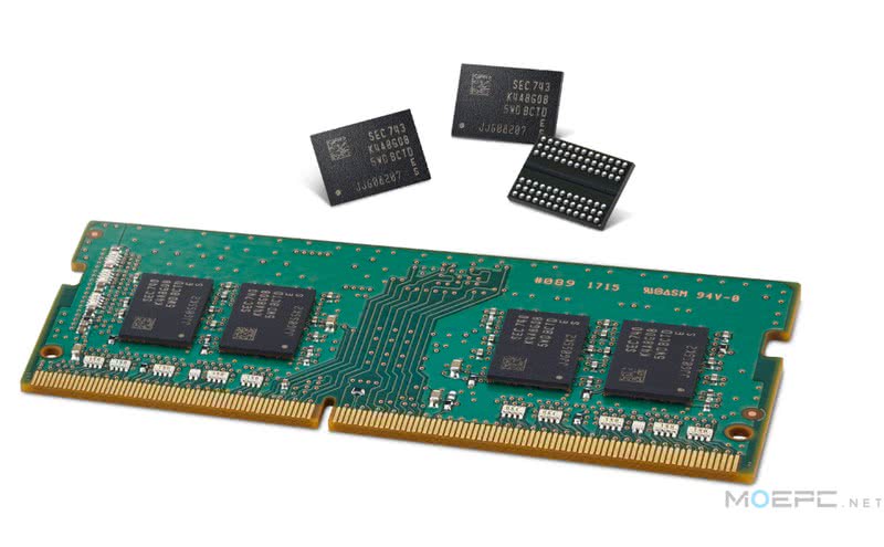
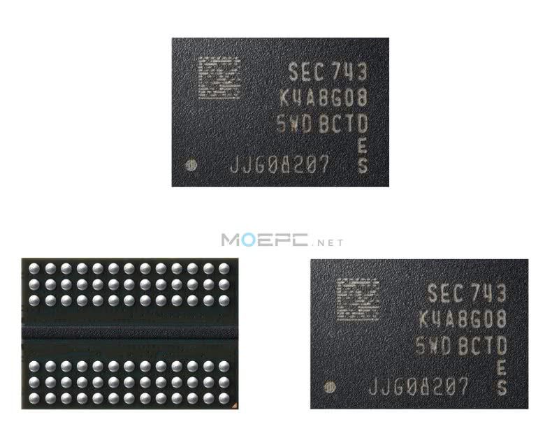
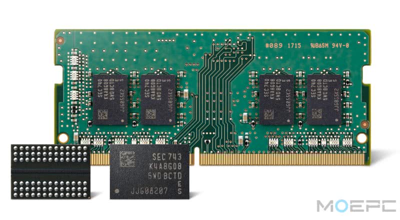
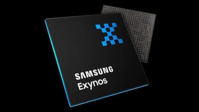
三星今天宣布,业界首款第二代1y-nm 8Gb DDR4 DRAM颗粒的量产已经开始。该款8Gb DDR4在同类型颗粒中拥有最高性能和能效,尺寸也最小。
三星称,相较第一代1x-nm 8Gb DDR4颗粒,第二代1y-nm将最大生产能力提高了约30%。与此同时,更先进的电路设计技术也把性能和能效提高了10-15%。还应用了一些新技术,包括高灵敏度数据感知系统和“air spacer”排列,这次没有使用EUV。【1x = 17-19nm;1y = 15nm;1z = 11-14nm】
新的8Gb DDR4可以运行在3600Mbps,上一代为3200Mbps【当然不是说特挑的三星B-Die】
三星正计划加速引入下一代DRAM颗粒,包括DDR5,HBM3,LPDDR5和GDDR6,为企业级服务器、移动设备、超算、高性能计算系统以及高端显卡提供存储。
本次发布的1y-nm DDR4 颗粒已经完成了和CPU厂商间的验证。PR中提到三星将提升1y-nm及1x-nm颗粒的产量。
PR原文:
Samsung Now Mass Producing Industry’s First 2nd-generation, 10-Nanometer Class DRAM
Korea on December 20, 2017
Samsung Electronics, the world leader in advanced memory technology, announced today that it has begun mass producing the industry’s first 2nd-generation of 10-nanometer class* (1y-nm), 8-gigabit (Gb) DDR4 DRAM. For use in a wide range of next-generation computing systems, the new 8Gb DDR4 features the highest performance and energy efficiency for an 8Gb DRAM chip, as well as the smallest dimensions.
“By developing innovative technologies in DRAM circuit design and process, we have broken through what has been a major barrier for DRAM scalability,” said Gyoyoung Jin, president of Memory Business at Samsung Electronics. “Through a rapid ramp-up of the 2nd-generation 10nm-class DRAM, we will expand our overall 10nm-class DRAM production more aggressively, in order to accommodate strong market demand and continue to strengthen our business competitiveness.”
Samsung’s 2nd-generation 10nm-class 8Gb DDR4 features an approximate 30 percent productivity gain over the company’s 1st?generation 10nm-class 8Gb DDR4. In addition, the new 8Gb DDR4’s performance levels and energy efficiency have been improved about 10 and 15 percent respectively, thanks to the use of an advanced, proprietary circuit design technology. The new 8Gb DDR4 can operate at 3,600 megabits per second (Mbps) per pin, compared to 3,200 Mbps of the company’s 1x-nm 8Gb DDR4.
To enable these achievements, Samsung has applied new technologies, without the use of an EUV process. The innovation here includes use of a high-sensitivity cell data sensing system and a progressive “air spacer” scheme.
In the cells of Samsung’s 2nd-generation 10nm-class DRAM, a newly devised data sensing system enables a more accurate determination of the data stored in each cell, which leads to a significant increase in the level of circuit integration and manufacturing productivity.
The new 10nm-class DRAM also makes use of a unique air spacer that has been placed around its bit lines to dramatically decrease parasitic capacitance**. Use of the air spacer enables not only a higher level of scaling, but also rapid cell operation.
With these advancements, Samsung is now accelerating its plans for much faster introductions of next-generation DRAM chips and systems, including DDR5, HBM3, LPDDR5 and GDDR6, for use in enterprise servers, mobile devices, supercomputers, HPC systems and high-speed graphics cards.
Samsung has finished validating its 2nd-generation 10nm-class DDR4 modules with CPU manufacturers, and next plans to work closely with its global IT customers in the development of more efficient next-generation computing systems.
In addition, the world’s leading DRAM producer expects to not only rapidly increase the production volume of the 2nd-generation 10nm-class DRAM lineups, but also to manufacture more of its mainstream 1st-generation 10nm-class DRAM, which together will meet the growing demands for DRAM in premium electronic systems worldwide.
* Editors’ Note 1: 10nm-class denotes a process technology node somewhere between 10 and 19 nanometers. Samsung launched its first DRAM product based on a 10nm-class process in February, 2016.
** Editors’ Note 2: Parasitic capacitance is unwanted capacitance that exists between the parts of an electronic circuit or electronic part, because of their proximity to each other. When two electrical conductors at different voltages are too close together, they are adversely affected by each other’s electric field and store opposite electric charges such as those produced by a capacitor.
本文地址:http://www.moepc.net/?post=3931
via:samsung
MOEPC.NET编译,转载请保留出处。
马文
“新的8Gb DDR4可以运行在3600(Mbps),上一代为3200(Mbps)” 是不是打错了?
RAM应该是以运行频率表示,单位应该是(MHz)。
@IAMPETER:看原文。
另外MHz也是错的
实际频率只有一半的1800MHz
要准确说应该是3600MT/s
原文是Mbps所以我写的Mbps
话说淘宝有三星cdie的条子了说是包上3200来着,以前不是说cdie做翻车了么,这批不知道是什么来路
感觉对ZEN是好事。
10nm内存颗粒
现在主流内存颗粒是多少nm?
14/16还是20?
@wangbaisen1990:17nm吧。记不清了。内存销量大都是用成熟和低成本工艺