【NVIDIA GTX1080 & 1070FE评测:FinFET世代的开端】NVIDIA GeForce GTX 1080 & GTX 1070 Founders Editions Review: Kicking Off the FinFET Generation
source:http://www.anandtech.com/show/10325/the-nvidia-geforce-gtx-1080-and-1070-founders-edition-review
先挖个坑,看得懂的就先看,看不懂的看图吧…..
因为1060和480的Review周五会出,优先翻译这俩
本篇有时间了会一点点翻译的…太长了?
在1080发布两个月、1070发布一个月后、Anandtech终于发布了这篇难产的评测。
与大多数媒体稍带浮躁的Day One Review不同,Anandtech更倾向于深入探索,更有研究的价值。

It has taken about 2 years longer than we’d normally see, but the next full generation of GPUs are finally upon us. Powered by FinFET based nodes at TSMC and GlobalFoundries, both NVIDIA and AMD have released new GPUs with new architectures built on new manufacturing nodes. AMD and NVIDIA did an amazing job making the best of 28nm over the 4 year stretch, but now at long last true renewal is at hand for the discrete GPU market.
Back in May we took a first look at the first of these cards, NVIDIA’s GeForce GTX 1080 Founders Edition. Launched at $700, it was immediately the flagship for the FinFET generation. Now today, at long (long) last, we will be taking a complete, in-depth look at the GTX 1080 Founders Edition and its sibling the GTX 1070 Founders Edition. Architecture, overclocking, more architecture, new memory technologies, new features, and of course copious benchmarks. So let’s get started on this belated look at the latest generation of GPUs and video cards from NVIDIA.

As a quick refresher, here are the specifications for the new cards. At a high level the Pascal architecture (as implemented in GP104) is a mix of old and new; it’s not a revolution, but it’s an important refinement. Maxwell as an architecture was very successful for NVIDIA both at the consumer level and the professional level, and for the consumer iterations of Pascal, NVIDIA has not made any radical changes. The basic throughput of the architecture has not changed ? the ALUs, texture units, ROPs, and caches all perform similar to how they did in GM2xx.
Consequently the performance aspects of consumer Pascal ? we’ll ignore GP100 for the moment ? are pretty easy to understand. NVIDIA’s focus on this generation has been on pouring on the clockspeed to push total compute throughput to 8.9 TFLOPs, and updating their memory subsystem to feed the beast that is GP104.
GeForce GTX 1080

The GeForce GTX 1080 is a fully enabled implementation of GP104. This means 2560 CUDA cores split up over 20 SMs operating at a blistering boost clock of 1733MHz. NVIDIA is positioning GTX 1080 as a full generational update over GTX 980, and thanks to a combination of a slightly wider GPU and a much faster clockspeed, they can generally deliver on this. By the numbers, GTX 1080 offers 78% more raw compute, texturing, and geometry performance, and 43% more ROP throughput. Of course the latter is as much a product of memory bandwidth as it is the ROPs themselves, and for that NVIDIA has some new memory technologies.
Feeding the beast that is GTX 1080 is 8GB of GDDR5X. A new memory standard that extends the effective memory bandwidth of GDDR5, GTX 1080’s GDDR5X runs at 10Gbps, and is attached to a 256-bit memory bus. This gives GTX 1080 a full 320GB/sec of memory bandwidth to play with, 43% more than GTX 980. And as we’ll see in the coming architectural pages, these raw numbers don’t factor in the architectural improvements that allow the Pascal GPUs to stretch their memory bandwidth even further.
Finally, GTX 1080’s TDP is rated at 180W. This is a slight increase from the past generation, where GTX 980 required 165W. Video card specifications are of course a sliding scale ? balancing desired performance with cooling capabilities and power consumption ? and ultimately NVIDIA has opted to eat a slight increase in power consumption to allow GTX 1080 to deliver more performance than it otherwise would.
GeForce GTX 1070
Meanwhile below the GTX 1080 we have its lower price and lower performance sibling, the GTX 1070. The standard high-end salvage part, GTX 1070 trades off fewer functional blocks and the lower resulting performance in exchange for a significantly lower price than the GTX 1080. From a hardware perspective, the GTX 1070 utilizes GP104 with 1 of the 4 Graphics Processing Clusters (GPCs) disabled. Relative to GTX 1080, this knocks off around 25% of the shading/texturing/compute performance. However the memory controllers and ROP partitions remain untouched. With this configuration NVIDIA is pitching the GTX 1070 as a full generational update to the GTX 970, and with any luck, the GTX 1070 will be as well accepted as its extremely successful predecessor.

All told then, GTX 1070 provides 1920 CUDA cores split up over 15 SMMs. Those 15 SMMs are in turn running at a base clockspeed of 1506MHz and a boost clock of 1683MHz. This is slightly lower than GTX 1080, but as we’ll see in our full benchmark section, the official clockspeeds have a very little impact; it’s the disabled GPC that really makes the difference. By the numbers, relative to the GTX 970 the GTX 1070 offers 65% more shading, texturing, and geometry throughput, and 63% more ROP throughput. The latter coming as a courtesy of both the higher clockspeeds and the fact that GTX 1070 ships with all 64 ROPs enabled, versus 56 of 64 on GTX 970.
As for memory, GTX 1070 doesn’t get GDDR5X. Instead the card gets 8GB of GDDR5 running at 8Gbps. This delivers a total memory bandwidth of 256GB/sec, and again unlike GTX 970, there is nothing going on with partitions here, so all of that memory and all of that bandwidth is operating in one contiguous partition, giving the GTX 1070 an effective memory bandwidth increase of 31%. GTX 1070 is the first NVIDIA card to ship with 8Gbps GDDR5, a memory speed I once didn’t think possible. NVIDIA and the memory partners are pushing GDDR5 to the limit by doing this, but at this point in time this is the most economical way to boost memory bandwidth without resorting to more exotic and expensive solutions like GDDR5X.
GTX 1070 is rated for a 150W TDP; this is a smaller, 5W increase over its predecessor. Despite the official TDP, it should be noted that NVIDIA is not pitching this card as their 150W champion for systems with a single 6-pin PCIe power cable, and it will require a more powerful 8-pin cable. For systems that need a true sub-150W card, this is where the GTX 1060 will step in. Otherwise NVIDIA is making a very interesting power play here what is now the second most powerful video card on the market does so on just 150W.
Cards, Pricing, & Availability
For the GTX 1000 series, NVIDIA has undertaken a significant change in how they handle reference boards and how those boards are priced. What were once reference boards are now being released as the Founders Edition boards. These boards are largely similar to NVIDIA’s last-generation reference boards, built using a standard PCB and NVIDA’s high-end blower cooler, along with some additional cooling upgrades. The Founders Edition cards will, in turn, not be sold at NVIDIA’s general MSRP for each family, but rather they will be sold as premium cards for around $80-$100 more.

As a result we have two prices to talk about. For the GTX 1080, the family MSRP is $599. At the base level this is a slight price increase over the GTX 980, which launched at $549. As the Founders Edition cards are not being sold at this price, it is instead being filled by semi and fully custom cards from NVIDIA’s partners. These custom cards offer a mix of designs, but at the cheapest level (those cards closest to the MSRP) we’re predominantly looking at dual fan open air cooled cards. The rest of the lineup is filled by more advanced cards (including some closed loop liquid coolers) with factory overclocks and other features that are sold at a premium price. The GTX 1080 Founders Edition card, for its part, fits in to this picture at $699, a $100 premium.

The story then is much the same for the GTX 1070. Its family MSRP is $379, which its Founders Edition counterpart is being sold for $449. At $379 for the family MSRP, this is a $40 price increase over the GTX 970, and I am curious over the long run whether this will significantly impact sales. One of the factors that made GTX 970 such a well-received card was its price, and this takes away from that by a bit. Otherwise, as with the GTX 1080, the partners’ custom cards for the GTX 1070 run the gamut from simple dual fan cards at the cheapest prices, up to premium, factory overclocked cards at the highest prices.


Unfortunately for everyone involved, the plan for pricing and reality haven’t quite agreed with each other. Even now, 2 months after the launch of the GTX 1080, card supplies are slim. There is effectively a shortage of GTX 1080 cards, as while NVIDIA insists they are continuing to ship out a good supply, those cards appear to be getting plucked off of virtual and physical shelves almost as quickly. As of the time this paragraph was written, Newegg only has a single GTX 1080 in stock, a Founders Edition card at $699.
For the last several generations it has been pretty common for the first batch or two of high-end cards to sell out, however to be sold out for 2 months is a lot less common. Other than NVIDIA’s Titan series card, which are a special case due to their prosumer market, I can’t immediately recall the last time an NVIDIA flagship card was this hard to get this late after a launch. For NVIDIA and its partners there are worse problems in the world ? it’s better to have too few cards than too many cards that you can’t sell ? but it certainly puts a damper on things for both the partners and for customers.
Meanwhile the GTX 1070 situation is noticeably better, though still not great. About half of the models that Newegg carries are in stock at any given time. So potential GTX 1070 owners have more options, though if they’re after a specific card they may find themselves waiting.

But the real problem with this shortage is that it has removed any incentive to keep prices close to NVIDIA’s MSRP. GTX 1070 prices start at $429 instead of $379, while GTX 1080 prices start at $649 (and if you actually want a card in stock, that’ll be $699). These are prices that are closer to last generations GTX 980 Ti/980 prices than they are 980/970, and it means that the actual GTX 1000 series price premium is much higher as it stands, at $100+ compared to the last generation. Given that these cards keep selling out, clearly there are enough buyers willing to pay these prices ? it’s the free market in action ? but it means NVIDIA’s MSRPs are for the moment an imaginary number. At this point all that we can do is hope that once the shortage breaks, there will be more intensive competition between the partners and retailers, and prices will fall down to MSRP.
As for the larger competitive landscape, as we’re looking at high-end cards at the start of a new generation, there really isn’t any competition to speak of. The GTX 1000 series sets a new bar for performance, and while last generation cards are being priced to clear out inventories, they aren’t performance competitive with the new cards. Meanwhile stalwart competitor AMD has opted to go after the mainstream market first rather than starting at the high-end. This means that the GTX 1080 and GTX 1070 will not have any competition for at least the next few months, leaving NVIDIA solely in the driver’s seat at the high-end, and in sole possession of the GPU performance crown.

Pascal’s Architecture: What Follows Maxwell
With the launch of a new generation of GPUs we’ll start things off where we always do: the architecture.
Discrete GPUs occupy an interesting space when it comes to the relationship between architecture and manufacturing processes. Whereas CPUs have architecture and manufacturing process decoupled ? leading to Intel’s aptly named (former) tick-tock design methodology ? GPUs have aligned architectures with manufacturing processes, with a new architecture premiering alongside a new process. Or rather, GPU traditionally did. Maxwell threw a necessary spanner into all of this, and in its own way Pascal follows this break from tradition.
As the follow-up to their Kepler architecture, with Maxwell NVIDIA introduced a significantly altered architecture, one that broke a lot of assumptions Kepler earlier made and in the process vaulted NVIDIA far forward on energy efficiency. What made Maxwell especially important from a development perspective is that it came not on a new manufacturing process, but rather on the same 28nm process used for Kepler two years earlier, and this is something NVIDIA had never done before. With the 20nm planar process proving unsuitable for GPUs and only barely suitable for SoCs ? the leakage from planar transistors this small was just too high ? NVIDIA had to go forward with 28nm for another two years. It would come down to their architecture team to make the best of the situation and come up with a way to bring a generational increase in performance without the traditional process node shrink.
Now in 2016 we finally have new manufacturing nodes with the 14nm/16nm FinFET processes, giving GPU manufacturers a long-awaited (and much needed) opportunity to bring down power consumption and reduce chip size through improved manufacturing technology. The fact that it has taken an extra two years to get here, and what NVIDIA did in the interim with Maxwell, has opened up a lot of questions about what would follow for NVIDIA. The GPU development process is not so binary or straightforward that NVIDIA designed Maxwell solely because they were going to be stuck on the 28nm process ? NVIDIA would have done Maxwell either way ? but it certainly was good timing to have such a major architectural update fall when it did.
So how does NVIDIA follow-up on Maxwell then? The answer comes in Pascal, NVIDIA’s first architecture for the FinFET generation. Designed to be built on TSMC’s 16nm process, Pascal is the latest and the greatest, and like every architecture before it is intended to further push the envelope on GPU performance, and ultimately push the envelope on the true bottleneck for GPU performance, energy efficiency.

HPC vs. Consumer: Divergence
Pascal is an architecture that I’m not sure has any real parallel on a historical basis. And a big part of that is because to different groups within NVIDIA, Pascal means different things and brings different things, despite the shared architecture. On the one side is the consumer market, which is looking for a faster still successor to what Maxwell delivered in 2014 and 2015. Meanwhile on the high performance compute side, Pascal is the long-awaited update to the Kepler architecture (Maxwell never had an HPC part), combining the lessons of Maxwell with the specific needs of the HPC market.

The result is that there’s an interesting divergence going on between the HPC side and its GP100 GPU, and the consumer side and the GP104 GPU underlying GTX 1080. Even as far back as Fermi there was a distinct line separating HPC-class GPUs (GF100) from consumer/general compute GPUs (GF104), but with Pascal this divergence is wider than ever before. Ultimately the HPC market and GP100 is beyond the scope of this article and I’ll pick it up in detail another time, but because NVIDIA announced GP100 before GP104, it does require a bit of addressing to help sort out what’s going on and what NVIDA’s design goals were with GP104.
Pascal as an overarching architecture contains a number of new features, however not all of those features are present in all SKUs. If you were to draw a Venn diagram of Pascal, what you would find is that the largest collection of features are found in GP100, whereas GP104, like the previous Maxwell architecture before it, is stripped down for speed and efficiency. As a result while GP100 has some notable feature/design elements for HPC ? things such faster FP64 & FP16 performance, ECC, and significantly greater amounts of shared memory and register file capacity per CUDA core ? these elements aren’t present in GP104 (and presumably, future Pascal consumer-focused GPUs).

Ultimately what we’re seeing in this divergence is a greater level of customization between NVIDIA’s HPC and consumer markets. The HPC side of NVIDIA is finally growing up, and it’s growing fast. The long term plan at NVIDIA has been to push GPU technology beyond consumer and professional graphics, and while it has taken years longer than NVIDIA originally wanted, thanks in big part to success in the deep learning market,NVIDIA is finally achieving their goals.
This means that although GP100 is a fully graphics capable GPU, it doesn’t necessarily have to be put into video cards to make sense for NVIDIA to manufacture, and as a result NVIDIA can make it even more compute focused than prior-generation parts like GK110 and GF110. And that in turn means that although this divergence is driven by the needs of the HPC market ? what features need to be added to make a GPU more suitable for HPC use cases ? from the perspective of the consumer market there is a tendency to perceive that consumer parts are falling behind. Especially with how GP100 and GP104’s SMs are differently partitioned.

This is a subject I’ll revisit in much greater detail in the future when we focus on GP100. But for now, especially for the dozen of you who’ve emailed over the past month asking about why the two are so different, the short answer is that the market needs for HPC are different from graphics, and the difference in how GP100 and GP104 are partitioned reflect this. GP100 and GP104 are both unequivocally Pascal, but GP100 gets smaller SM partitions in order to increase the number of registers and the amount of shared memory available per CUDA core. Shared memory and register contention on graphics workloads isn’t nearly as great as with HPC tasks ? pixel shader threads are relatively short and independent from each other ? which means that while the increased ratios benefit HPC workloads, for graphics the gains would be minimal. And the costs to power and die space would, in turn, far outweigh any benefits.
GP104: The Heart of GTX 1080
At the heart of the GTX 1080 is the first of the consumer-focused Pascal GPUs, GP104. Though no two GPU generations are ever quite alike, GP104 follows a number of design cues established with the past couple 104 GPUs. Overall 104 GPUs have struck a balance between size and performance, allowing NVIDIA to get a suitably high yielding GPU out at the start of a generation, and to be followed up with larger GPUs later on as yields improve. With the exception of the GTX 780, 104 GPUs been the backbone of NVIDIA’s GTX 70 and 80 parts, and that is once again the case for the Pascal generation.

In terms of die size, GP104 comes in at 314mm2. This is right in NVIDIA’s traditional sweet spot for these designs, slotting in between the 294mm2 GK104 and the 332mm2 GF104. In terms of total transistors we’re looking at 7.2B transistors, up from 3.5B on GK104 and the 5.2B of the more unusual GM204. The significant increase in density comes from the use of TSMC’s 16nm FinFET process, which compared to 28nm combines a full node shrink, something that has been harder and harder to come by as the years have progressed.

Though the density improvement offered by TSMC’s 16nm process is of great importance to GP104’s overall performance, for once density takes a back seat to the properties of the process itself. I am of course speaking about the FinFET transistors, which are the headlining feature of TSMC’s process.
We’ve covered FinFET technology in depth before, so I won’t completely rehash it here. But in brief, FinFETs are an important development for chip fabrication as processes have gone below 28nm. As traditional, planar transistors have shrunk in feature size ? and ultimately, the number of atoms they’re comprised of ? electrical leakage has increased. With fewer atoms in a transistor, there are equally fewer atoms to control the flow of electrons.
FinFET in turn is a solution to this problem, essentially allowing fabs to turn back the clock on electrical leakage. By building transistors as three-dimensional objects with height as opposed to two-dimensional objects, giving FinFET transistors their characteristic fins in the process, FinFET technology greatly reduces the amount of energy a transistor leaks. In practice what this means is that FinFET technology not only reduces the total amount of energy wasted from leakage, but it also allows transistors to be operated at a much lower voltage, something we’ll see in depth with our analysis of GTX 1080.

FinFETs, or rather the lack thereof, are a big part of why we never saw GPUs built on TSMC’s 20nm process. It was TSMC’s initial belief that they could contain leakage well enough using traditional High-K Metal Gate (HKMG) technology on 20nm, a bet they ultimately lost. At 20nm, planar transistors were just too leaky to use for many applications, which is why ultimately we only saw SoCs on 20nm (and even then they were suboptimal). FinFETs, as it turns out, are absolutely necessary to get good performance out of transistors built on processes below 28nm.
And while it took TSMC some time to get there, now that they have the capability NVIDIA can reap the benefits. Not only can NVIDIA finally build a relatively massive chip like a GPU on a sub-28nm process, but thanks to the various beneficial properties of FinFETs, it allows them to take their designs in a different direction than what they could do on 28nm.
GP104’s Architecture
Looking at an architecture diagram for GP104, Pascal ends up looking a lot like Maxwell, and this is not by chance. After making more radical changes to their architecture with Maxwell, for Pascal NVIDIA is taking a bit of a breather. Which is not to say that Pascal is Maxwell on 16nm ? this is very much a major feature update ? but when it comes to discussing the core SM architecture itself, there is significant common ground with Maxwell.

We’ll start with the GP104 SM. Simply named the SM for this generation ? NVIDIA has ditched the generational suffix due to the potential for confusion with the used-elsewhere SMP ? the GP104 SM is very similar to the Maxwell SM. We’re still looking at a single SM partially sub-divided into four pieces, each containing a single warp scheduler that’s responsible for feeding 32 CUDA cores, 8 load/store units, and 8 Special Function Units, backed by a 64KB register file. There are two dispatch ports per warp schedule, so when an instruction stream allows it, a warp scheduler can extract a limited amount of ILP with an instruction stream by issuing a second instruction to an unused resource.

Meanwhile shared between every pair of sub-partitions is 4 texture units and the combined L1/texture cache, again unchanged from Maxwell. Finally, we have the resources shared throughout the whole SM: the 96KB shared memory, the instruction cache, and not pictured on NVIDIA’s diagrams, the 4 FP64 CUDA cores and 1 FP16x2 CUDA core.
Overall then at the diagram level the GP104 SM looks almost identical to the Maxwell SM, but with one exception: the PolyMorph Engine. Although the distinction is largely arbitrary for GP104, the PolyMorph Engine has been moved up a level; it’s no longer part of the SM, but rather part of the newly re-introduced TPC, which itself sits between the GPC and the SM.
The TPC exists because although GP104 still has a 1:1 ratio between PolyMorph Engines and SMs, the Pascal architecture itself allows for different SM configurations, which is in turn used on GP100 to allow it to have multiple smaller SMs of 64 CUDA Cores. For GP100 the TPC allows for multiple SMs to share a PolyMorph Engine, but for GP104 there’s no sharing involved. To that end the TPC as an organizational unit technically exists across all Pascal parts, but it has no real significance for GP104. In fact it doesn’t even have a real name; NVIDIA reused the acronym from earlier DX10 architectures, where the TPC was the name assigned to the Texture Processor Cluster.
Looking at the bigger picture of the complete GP104 GPU, the similarities continue between GP104 and GM204. GP104’s SMs are clustered five-a-piece inside of the GPC, with each cluster sharing a single Raster Engine. Overall there are 4 such GPCs, giving us 20 SMs altogether. Compared to GM204 then, we’re looking at the same number of GPCs, with each GPC having gained 1 SM.
Things get more interesting when we look at the back end of the rendering/execution pipeline, which is comprised of the L2 cache, ROPs, and memory controllers. The ROP/L2 count has not changed relative to GM204 ? we still have 64 ROPs paired up with a total of 2MB of L2 cache ? however the memory controller count has. And with it the logical configuration of the ROP/L2 blocks have changed as well.
Whereas GM204 had 4 64bit GDDR5 memory controllers, each connected to 2 or 4 memory chips, GP104 breaks that down further to 8 32bit GDDR5X memory controllers, each of which is connected to 1 memory chip on GTX 1080. I’ll go into greater detail on GDDR5X a bit later, but the significance of this backend organizational change has to do with the introduction of GDDR5X. Because GDDR5X reads and writes data in 64B amounts (versus 32B amounts on GDDR5), NVIDIA has reorganized the memory controllers to ensure that each memory controller still operates on the same amount of data. With GDDR5 they teamed up two GDDR5 channels to get 64B operations, whereas with GDDR5X this can be accomplished with a single memory channel.
This in turn is where the ROP reorganization comes from. As there’s a 1:1 relationship between ROP partitions and memory controllers, the 64 ROPs are now broken up into 8 partitions for GP104, as opposed to 4 partitions on GM204. There are some performance tradeoffs that come from having more ROP partitions, but to the best of my knowledge these should not be significant.
Meanwhile the new GDDR5X memory controllers are also backwards compatible with traditional GDDR5, which in turn is used to drive the GTX 1070 with its 8Gbps GDDR5. The difference in operation between GDDR5 and GDDR5X does make the ROP situation a bit trickier overall for NVIDIA’s architects ? now they need to be able to handle two different memory access patterns ? though for NVIDIA this isn’t a wholly new problem. Previous generation architectures have supported both GDDR5 and DDR3, the two of which have their own differences in memory access patterns.
In a by-the-numbers comparison then, Pascal does not bring any notable changes in throughput relative to Maxwell. CUDA cores, texture units, PolyMorph Engines, Raster Engines, and ROPs all have identical theoretical throughput-per-clock as compared to Maxwell. So on a clock-for-clock, unit-for-unit basis, Pascal is not any faster on paper. And while NVIDIA does not disclose the size/speed of most of their internal datapaths, so far I haven’t seen anything to suggest that these have radically changed. This continuity means that outside of its new features, GP104 behaves a lot like GM204. Though it should be noted that real world efficiency isn’t quite as cut and dry, as various factors such as the increased SM count and changes in memory technology can greatly influence this.
FP16 Throughput on GP104: Good for Compatibility (and Not Much Else)
Speaking of architectural details, I know that the question of FP16 (half precision) compute performance has been of significant interest. FP16 performance has been a focus area for NVIDIA for both their server-side and client-side deep learning efforts, leading to the company turning FP16 performance into a feature in and of itself.
Starting with the Tesla X1 ? and then carried forward for Pascal ? NVIDIA added native FP16 compute support to their architectures. Prior to these parts, any use of FP16 data would require that it be promoted to FP32 for both computational and storage purposes, which meant that using FP16 did not offer any meaningful improvement in performance or storage needs. In practice this meant that if a developer only needed the precision offered by FP16 compute (and deep learning is quickly becoming the textbook example here), that at an architectural level power was being wasted computing that extra precision.
Pascal, in turn, brings with it native support for FP16 compute for both storage and compute. On the storage side, Pascal supports FP16 datatypes, with relative to the previous use of FP32 means that FP16 values take up less space at every level of the memory hierarchy (registers, cache, and DRAM). On the compute side, Pascal introduces a new type of FP32 CUDA core that supports a form of FP16 execution where two FP16 operations are run through the CUDA core at once (vec2). This core, which for clarity I’m going to call an FP16x2 core, allows the GPU to process 1 FP32 or 2 FP16 operations per clock cycle, essentially doubling FP16 performance relative to an identically configured Maxwell or Kepler GPU.

Now there are several special cases here due to the use of vec2 ? packing together operations is not the same as having native FP16 CUDA cores ? but in a nutshell NVIDIA can pack together FP16 operations as long as they’re the same operation, e.g. both FP16s are undergoing addition, multiplication, etc. Fused multiply-add (FMA/MADD) is also a supported operation here, which is important for how frequently it is used and is necessary to extract the maximum throughput out of the CUDA cores.
Low precision operations are in turn seen by NVIDIA as one of the keys into further growing their increasingly important datacenter market, as deep learning and certain other tasks are themselves rapidly growing fields. Pascal isn’t just faster than Maxwell overall, but when it comes to FP16 operations on the FP16x2 core, Pascal is a lot faster, with theoretical throughput over similar Maxwell GPUs increasing by over three-fold thanks to the combination of overall speed improvements and double speed FP16 execution.
GeForce GTX 1080, on the other hand, is not faster at FP16. In fact it’s downright slow. For their consumer cards, NVIDIA has severely limited FP16 CUDA performance. GTX 1080’s FP16 instruction rate is 1/128th its FP32 instruction rate, or after you factor in vec2 packing, the resulting theoretical performance (in FLOPs) is 1/64th the FP32 rate, or about 138 GFLOPs.

After initially testing FP16 performance with SiSoft Sandra ? one of a handful of programs with an FP16 benchmark built against CUDA 7.5 ? I reached out to NVIDIA to confirm whether my results were correct, and if they had any further explanation for what I was seeing. NVIDIA was able to confirm my findings, and furthermore that the FP16 instruction rate and throughput rates were different, confirming in a roundabout manner that GTX 1080 was using vec2 packing for FP16.
As it turns out, when it comes to FP16 NVIDIA has made another significant divergence between the HPC-focused GP100, and the consumer-focused GP104. On GP100, these FP16x2 cores are used throughout the GPU as both the GPU’s primarily FP32 core and primary FP16 core. However on GP104, NVIDIA has retained the old FP32 cores. The FP32 core count as we know it is for these pure FP32 cores. What isn’t seen in NVIDIA’s published core counts is that the company has built in the FP16x2 cores separately.
To get right to the point then, each SM on GP104 only contains a single FP16x2 core. This core is in turn only used for executing native FP16 code (i.e. CUDA code). It’s not used for FP32, and it’s not used for FP16 on APIs that can’t access the FP16x2 cores (and as such promote FP16 ops to FP32). The lack of a significant number of FP16x2 cores is why GP104’s FP16 CUDA performance is so low as listed above. There is only 1 FP16x2 core for every 128 FP32 cores.
Limiting the performance of compute-centric features in consumer parts is nothing new for NVIDIA. FP64 has been treated as a Tesla feature since the beginning, and consumer parts have either shipped with a very small number of FP64 CUDA cores for binary compatibility purposes, or when a GeForce card uses an HPC-class GPU, FP64 performance is artificially restricted. This allows NVIDIA to include a feature for software development purposes while enforcing strict market segmentation between the GeForce and Tesla products. However in the case of FP64, performance has never been slower than 1/32, whereas with FP16 we’re looking at a much slower 1/128 instruction rate. Either way, the end result is that like GP104’s FP64 support, GP104’s FP16 support is almost exclusively for CUDA development compatibility and debugging purposes, not for performant consumer use.

As for why NVIDIA would want to make FP16 performance so slow on Pascal GeForce parts, I strongly suspect that the Maxwell 2 based GTX Titan X sold too well with compute users over the past 12 months, and that this is NVIDIA’s reaction to that event. GTX Titan X’s FP16 and FP32 performance was (per-clock) identical its Tesla equivalent, the Tesla M40, and furthermore both cards shipped with 12GB of VRAM. This meant that other than Tesla-specific features such as drivers and support, there was little separating the two cards.
The Titan series has always straddled the line between professional compute and consumer graphics users, however if it veers too far into the former then it puts Tesla sales at risk. Case in point: at this year’s NVIDIA GPU Technology Conference, I was approached twice by product vendors who were looking for more Titan X cards for their compute products, as at that time the Titan X was in short supply. Suffice it to say, Titan X has been very popular with the compute crowd.
In any case, limiting the FP16 instruction rate on GeForce products is an easy way to ensure that these products don’t compete with the higher margin Tesla business. NVIDIA has only announced one Tesla so far ? the high-end P100 ? but even that sold out almost immediately. For now I suspect that NVIDIA wants to ensure that P100 and M40 sales are not impacted by the new GeForce cards.
Overall I’m not surprised that NVIDIA limited the FP16 performance of the GTX 1080 ? albeit by a new record ? as they clearly consider faster FP16 performance a feature that can be monetized under Tesla. However I have to admit that I am surprised that NVIDIA limited it in hardware on GP104 in this fashion, similar to how they limit FP64 performance, rather than using FP16x2 cores throughout the GPU and using software cap. The difference is that had NVIDIA implemented a complete fast FP16 path in GP104 and merely turned it off for GeForce, then they could have used GP104 for high performance (and high margin) FP16 Tesla cards. However by building GP104 from the get-go with a single FP16x2 unit per SM, they have closed the door on that option.
Where things may get especially interesting when it comes to FP16 performance is in smaller-still chips such as GP106. NVIDIA admittedly never used GM204 as a high performance compute part ? it was used in the virtualization focused Tesla M6 and M60 cards ? but NVIDIA did produce a small form factor compute and deep learning focused card with the GM206 based Tesla M4. I fully expect that NVIDIA will want a successor to this card, which will be hard to do if only GP100 has fast FP16 support. At the same time NVIDIA has still yet to disclose the dGPUs used with the DRIVE PX 2 module, where again fast FP16 support is useful for neural network inference. It may very well be that GP104’s low hardware FP16 performance is something that is not shared by the rest of the Pascal consumer GPU family.
Designing GP104: Running Up the Clocks
So if GP104’s per-unit throughput is identical to GM204, and the SM count has only been increased from 2048 to 2560 (25%), then what makes GTX 1080 60-70% faster than GTX 980? The answer there is that instead of vastly increasing the number of functional units for GP104 or increasing per-unit throughput, NVIDIA has instead opted to significantly raise the GPU clockspeed. And this in turn goes back to the earlier discussion on TSMC’s 16nm FinFET process.
With every advancement in fab technology, chip designers have been able to increase their clockspeeds thanks to the basic physics at play. However because TSMC’s 16nm node adds FinFETs for the first time, it’s extra special. What’s happening here is a confluence of multiple factors, but at the most basic level the introduction of FinFETs means that the entire voltage/frequency curve gets shifted. The reduced leakage and overall “stronger” FinFET transistors can run at higher clockspeeds at lower voltages, allowing for higher overall clockspeeds at the same (or similar) power consumption. We see this effect to some degree with every node shift, but it’s especially potent when making the shift from planar to FinFET, as has been the case for the jump from 28nm to 16nm.
Given the already significant one-off benefits of such a large jump in the voltage/frequency curve, for Pascal NVIDIA has decided to fully embrace the idea and run up the clocks as much as is reasonably possible. At an architectural level this meant going through the design to identify bottlenecks in the critical paths ? logic sections that couldn’t run at as high a frequency as NVIDIA would have liked ? and reworking them to operate at higher frequencies. As GPUs typically (and still are) relatively low clocked, there’s not as much of a need to optimize critical paths in this matter, but with NVIDIA’s loftier clockspeed goals for Pascal, this changed things.

From an implementation point of view this isn’t the first time that NVIDIA has pushed for high clockspeeds, as most recently the 40nm Fermi architecture incorporated a double-pumped shader clock. However this is the first time NVIDIA has attempted something similar since they reined in their power consumption with Kepler (and later Maxwell). Having learned their lesson the hard way with Fermi, I’m told a lot more care went into matters with Pascal in order to avoid the power penalties NVIDIA paid with Fermi, exemplified by things such as only adding flip-flops where truly necessary.
Meanwhile when it comes to the architectural impact of designing for high clockspeeds, the results seem minimal. While NVIDIA does not divulge full information on the pipeline of a CUDA core, all of the testing I’ve run indicates that the latency (in clock cycles) of the CUDA cores is identical to Maxwell. Which goes hand in hand with earlier observations about throughput. So although optimizations were made to the architecture to improve clockspeeds, it doesn’t look like NVIDIA has made any more extreme optimizations (e.g. pipeline lengthening) that detectably reduces Pascal’s per-clock performance.

Finally, more broadly speaking, while this is essentially a one-time trick for NVIDIA, it’s an interesting route for them to go. By cranking up their clockspeeds in this fashion, they avoid any real scale-out issues, at least for the time being. Although graphics are the traditional embarrassingly parallel problem, even a graphical workload is subject to some degree of diminishing returns as GPUs scale farther out. A larger number of SMs is more difficult to fill, not every aspect of the rendering process is massively parallel (shadow maps being a good example), and ever-increasing pixel shader lengths compound the problem. Admittedly NVIDIA’s not seeing significant scale-out issues quite yet, but this is why GTX 980 isn’t quite twice as fast as GTX 960, for example.
Just increasing the clockspeed, comparatively speaking, means that the entire GPU gets proportionally faster without shifting the resource balance; the CUDA cores are 43% faster, the geometry frontends are 43% faster, the ROPs are 43% faster, etc. The only real limitation in this regard isn’t the GPU itself, but whether you can adequately feed it. And this is where GDDR5X comes into play.
Feeding Pascal: GDDR5X
An ongoing problem for every generation of GPUs is the matter of memory bandwidth. As graphics is an embarrassingly parallel problem, it scales out with additional ALUs ? and consequently Moore’s Law ? relatively well. Each successive generation of GPUs are wider and higher clocked, consuming more data than ever before.
The problem for GPUs is that while their performance tracks Moore’s Law well, the same cannot be said for DRAM. To be sure, DRAM has gotten faster over the years as well, but it hasn’t improved at nearly the same pace as GPUs, and physical limitations ensure that this will continue to be the case. So with every generation, GPU vendors need to be craftier and craftier about how they get more memory bandwidth, and in turn how they use that memory bandwidth.
To help address this problem, Pascal brings to the table two new memory-centric features. The first of which is support for the newer GDDR5X memory standard, which looks to address the memory bandwidth problem from the supply side.
By this point GDDR5 has been with us for a surprisingly long period of time ? AMD first implemented it on the Radeon HD 4870 in 2008 ? and it has been taken to higher clockspeeds than originally intended. Today’s GeForce GTX 1070 and Radeon RX 480 cards ship with 8Gbps GDDR5, a faster transfer rate than the originally envisioned limit of 7Gbps. That GPU manufacturers and DRAM makers have been able to push GDDR5 so high is a testament to their abilities, but at the same time the technology is clearly reaching its apex (at least for reasonable levels of power consumption)
As a result there has been a great deal of interest in the memory technologies that would succeed GDDR5. At the high end, last year AMD became the first vendor to implement version 1 of High Bandwidth Memory, a technology that is a significant departure from traditional DRAM and uses an ultra-wide 4096-bit memory bus to provide enormous amounts of bandwidth. Not to be outdone, NVIDIA has adopted HBM2 for their HPC-centric GP100 GPU, using it to deliver 720GB/sec of bandwidth for Pascal P100.
While from a technical level HBM is truly fantastic next-generation technology ? it uses cutting edge technology throughput, from TSV die-stacking to silicon interposers that connect the DRAM stacks to the processor ? its downside is that all of this next-generation technology is still expensive to implement. Precise figures aren’t publicly available, but the silicon interposer is more expensive than a relatively simple PCB, and connecting DRAM dies through TSVs and stacking them is more complex than laying down BGA DRAM packages on a PCB. For NVIDIA, a more cost-effective solution was desired for GP104.
That solution came from Micron and the JEDEC in the form of GDDR5X. A sort of half-generation extension of traditional GDDR5, GDDR5X further increases the amount of memory bandwidth available from GDDR5 through a combination of a faster memory bus coupled with wider memory operations to read and write more data from DRAM per clock. And though it’s not without its own costs such as designing new memory controllers and boards that can accommodate the tighter requirements of the GDDR5X memory bus, GDDR5X offers a step in performance between the relatively cheap and slow GDDR5, and relatively fast and expensive HBM2.

Relative to GDDR5, the significant breakthrough on GDDR5X is the implementation of Quad Data Rate (QDR) signaling on the memory bus. Whereas GDDR5’s memory bus would transfer data twice per write clock (WCK) via DDR, GDDR5X extends this to four transfers per clock. All other things held equal, this allows GDDR5X to transfer twice as much data per clock as GDDR5.

QDR itself is not a new innovation ? Intel implemented a quad pumped bus 15 years ago for the Pentium 4 with AGTL+ ? but this is the first time it has been implemented in a common JEDEC memory standard. The history of PC memory standards is itself quite a tale, and I suspect that the fact we’re only seeing a form of QDR now is related to patents. But regardless, here we are.
Going hand-in-hand with the improved transfer rate of the GDDR5X memory bus, GDDR5X also once again increases the size of read/write operations, as the core clockspeed of GDDR5X chips is only a fraction of the bus speed. GDDR5X uses a 16n prefetch, which is twice the size of GDDR5’s 8n prefetch. This translates to 64B reads/writes, meaning that GDDR5X memory chips are actually fetching (or writing) data in blocks of 64 bytes, and then transmitting it over multiple cycles of the memory bus. As discussed earlier, this change in the prefetch size is why the memory controller organization of GP104 is 8x32b instead of 4x64b like GM204, as each memory controller can now read and write 64B segments of data via a single memory channel.

Overall GDDR5X is planned to offer enough bandwidth for at least the next couple of years. The current sole supplier of GDDR5X, Micron, is initially developing GDDR5X from 10 to 12Gbps, and the JEDEC has been talking about taking that to 14Gbps. Longer term, Micron thinks the technology can hit 16Gbps, which would be a true doubling of GDDR5’s current top speed of 8Gbps. With that said, even with a larger 384-bit memory bus (ala GM200) this would only slightly surpass what kind of bandwidth HBM2 offers today, reinforcing the fact that GDDR5X will fill the gap between traditional GDDR5 and HBM2.
Meanwhile when it comes to power consumption and power efficiency, GDDR5X will turn back the clock, at least a bit. Thanks in large part to a lower operating voltage of 1.35v, circuit design changes, and a smaller manufacturing node for the DRAM itself, 10Gbps GDDR5X only requires as much power as 7Gbps GDDR5. This means that relative to GTX 980, GTX 1080’s faster GDDR5X is essentially “free” from a power perspective, not consuming any more power than before, according to NVIDIA.
That said, while this gets NVIDIA more bandwidth for the same power ? 43% more, in fact ? NVIDIA has now put themselves back to where they were with GTX 980. GDDR5X can scale higher in frequency, but doing so will almost certainly further increase power consumption. As a result they are still going to have to carefully work around growing memory power consumption if they continue down the GDDR5X path for future, faster cards.

On a final specification note, GDDR5X also introduces non-power-of-two memory chip capacities such as 12Gb. These aren’t being used for GTX 1080 ? which uses 8Gb chips ? but I wouldn’t be surprised if we see these used down the line. The atypical sizing would allow NVIDIA to offer additional memory capacities without resorting to asymmetrical memory configurations as is currently the case, all the while avoiding the bandwidth limitations that can result from that.

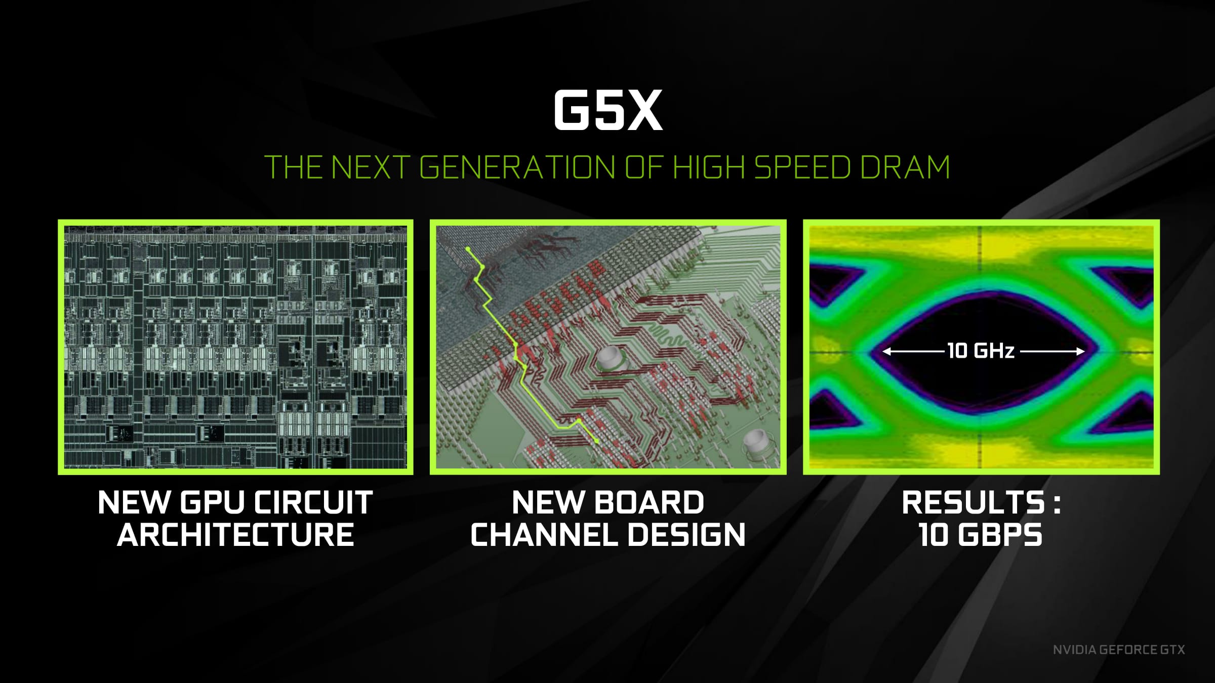
Moving on to implementation details, GP104 brings with it a new memory controller design to support GDDR5X. As intended with the specification, this controller design is backwards compatible with traditional GDDR5, and will allow NVIDIA to support both memory standards. At this point NVIDIA hasn’t talked about what kinds of memory speeds their new controller can ultimately hit, but the cropped signal analysis diagram published in their slide deck shows a very tight eye. Given the fact that NVIDIA’s new memory controller can operate at 8Gbps in GDDR5 mode, I would be surprised if we don’t see at least 12Gbps GDDR5X by the tail-end of Pascal’s lifecycle.
But perhaps the bigger challenge is on the board side of matters, where NVIDIA and their partners needed to develop PCBs capable of handling the tighter signaling requirements of the GDDR5X memory bus. At this point video cards are moving 10Gbps/pin over a non-differential bus, which is itself a significant accomplishment. And keep in mind that in the long run, the JEDEC and Micron want to push this higher still.
To that end it somewhat undersells the whole process to just say that GDDR5X required “tighter signaling requirements”, but it’s an apt description. There is no single technology in place on the physical trace side to make this happen; it’s just a lot of precision, intensive work into ensuring that the traces and the junctions between the PCB, the chip, and the die all retain the required signal integrity. With a 256-bit wide bus we’re not looking at something too wide compared to the 384 and 512-bit buses uses on larger GPUs, so the task is somewhat simpler in that respect, but it’s still quite a bit of effort to minimize the crosstalk and other phenomena that degrade the signal, and which GDDR5X has little tolerance for.
As it stands I suspect we have not yet seen the full ramifications of the tighter bus requirements, and we probably won’t for cards that use the reference board or the memory design lifted from the reference board. For stability reasons, data buses are usually overengineered, and it’s likely the GDDR5X memory itself that’s holding back overclocking. Things will likely get more interesting if and when GDDR5X filters its way down to cheaper cards, where keeping costs in check and eking out higher margins becomes more important. Alternatively, as NVIDIA’s partners get more comfortable with the tech and its requirements, it’ll be interesting to see where we end up with the ultra-high-end overclocking cards ?the Kingpins, Lightnings, Matrices, etc ? and whether all of the major partners can keep up in that race.
Feeding Pascal, Cont: 4th Gen Delta Color Compression
Now that we’ve seen GDDR5X in depth, let’s talk about the other half of the equation when it comes to feeding Pascal: delta color compression.
NVIDIA has utilized delta color compression for a number of years now. However the technology only came into greater prominence in the previous Maxwell 2 generation, when NVIDIA disclosed delta color compression’s existence and offered a basic overview of how it worked. As a reminder, delta color compression is a per-buffer/per-frame compression method that breaks down a frame into tiles, and then looks at the differences between neighboring pixels ? their deltas. By utilizing a large pattern library, NVIDIA is able to try different patterns to describe these deltas in as few pixels as possible, ultimately conserving bandwidth throughout the GPU, not only reducing DRAM bandwidth needs, but also L2 bandwidth needs and texture unit bandwidth needs (in the case of reading back a compressed render target).
Since its inception NVIDIA has continued to tweak and push the technology for greater compression and to catch patterns they missed on prior generations, and Pascal in that respect is no different. With Pascal we get the 4th generation of the technology, and while there’s nothing radical here compared to the 3rd generation, it’s another element of Pascal where there has been an iterative improvement on the technology.

New to Pascal is a mix of improved compression modes and new compression modes. 2:1 compression mode, the only delta compression mode available up through the 3rd generation, has been enhanced with the addition of more patterns to cover more scenarios, meaning NVIDIA is able to 2:1 compress blocks more often.
Meanwhile, new to delta color compression with Pascal is 4:1 and 8:1 compression modes, joining the aforementioned 2:1 mode. Unlike 2:1 mode, the higher compression modes are a little less straightforward, as there’s a bit more involved than simply the pattern of the pixels. 4:1 compression is in essence a special case of 2:1 compression, where NVIDIA can achieve better compression when the deltas between pixels are very small, allowing those differences to be described in fewer bits. 8:1 is more radical still; rather an operating on individual pixels, it operates on multiple 2×2 blocks. Specifically, after NVIDIA’s constant color compressor does its job ? finding 2×2 blocks of identical pixels and compressing them to a single sample ? the 8:1 delta mode then applies 2:1 delta compression to the already compressed blocks, achieving the titular 8:1 effective compression ratio.
Overall, delta color compression represents one of the interesting tradeoffs NVIDIA has to make in the GPU design process. The number of patterns is essentially a function of die space, so NVIDIA could always add more patterns, but would the memory bandwidth improvements be worth the real cost of die space and the power cost of those transistors? Especially since NVIDIA has already implemented the especially common patterns, which means new patterns likely won’t occur as frequently. NVIDIA of course pushed ahead here, thanks in part to the die and power savings of 16nm FinFET, but it gives us an idea of where they might (or might not) go in future generations in order to balance the costs and benefits of the technology, with less of an emphasis on patterns and instead making more novel use of those patterns.

To put all of this in numbers, NVIDIA pegs the effective increase in memory bandwidth from delta color compression alone at 20%. The difference is of course per-game, as the effectiveness of the tech depends on how well a game sticks to patterns (and if you ever create a game with random noise, you may drive an engineer or two insane), but 20% is a baseline number for the average. Meanwhile for anyone keeping track of the numbers over Maxwell 2, this is a bit less than the gains with NVIDIA’s last generation architecture, where the company claimed the average gain was 25%.
The net impact then, as NVIDIA likes to promote it, is a 70% increase in the total effective memory bandwidth. This comes from the earlier 40% (technically 42.9%) actual memory bandwidth gains in the move from 7Gbps GDDR5 to 10Gbps GDDR5X, coupled with the 20% effective memory bandwidth increase from delta compression. Keep those values in mind, as we’re going to get back to them in a little bit.

Meanwhile from a graphical perspective, to showcase the impact of delta color compression, NVIDIA sent over a pair of screenshots for Project Cars, colored to show what pixels had been compressed. Shown in pink, even Maxwell can compress most of the frame, really only struggling with finer details such as the trees, the grass, and edges of buildings. Pascal, by comparison, gets most of this. Trees and buildings are all but eliminated as visually distinct uncompressed items, leaving only patches of grass and indistinct fringe elements. It should be noted that these screenshots have most likely been picked because they’re especially impressive ? seeing as how not all games compress this well ? but it’s none the less a potent example of how much of a frame Pascal can compress.


Finally, while we’re on the subject of compress, I want to talk a bit about memory bandwidth relative to other aspects of the GPU. While Pascal (in the form of GTX 1080) offers 43% more raw memory bandwidth than GTX 980 thanks to GDDR5X, it’s important to note just how quickly this memory bandwidth is consumed. Thanks to GTX 1080’s high clockspeeds, the raw throughput of the ROPs is coincidentally also 43% higher. Or we have the case of the CUDA cores, whose total throughput is 78% higher, shooting well past the raw memory bandwidth gains.
While it’s not a precise metric, the amount of bandwidth available per FLOP has continued to drop over the years with NVIDIA’s video cards. GTX 580 offered just short of 1 bit of memory bandwidth per FLOP, and by GTX 980 this was down to 0.36 bits/FLOP. GTX 1080 is lower still, now down to 0.29bits/FLOP thanks to the increase in both CUDA core count and frequency as afforded by the 16nm process.

The good news here is that at least for graphical tasks, the CUDA cores generally aren’t the biggest consumer of DRAM bandwidth. That would fall to the ROPs, which are packed alongside the L2 cache and memory controllers for this very reason. In that case GTX 1080’s bandwidth gains keep up with the ROP performance increase, but only by just enough.
The overall memory bandwidth needs of GP104 still outpace the memory bandwidth gains from GDDR5X, and this is why features such as delta color compression are so important to GP104’s performance. GP104 is perpetually memory bandwidth starved ? adding more memory bandwidth will improve performance, as we’ll see in our overclocking results ? and that means that NVIDIA will continue to try to conserve memory bandwidth usage as much as possible through compression and other means. How long they can fight this battle remains to be seen ? they already encounter diminishing returns in some cases ? but in the meantime this allows NVIDIA to utilize smaller memory buses, keeping down the die size and power costs of their GPUs, making PCB costs cheaper, and of course boosting profit margins at the same time.
Asynchronous Concurrent Compute: Pascal Gets More Flexible
Continuing our dive into the Pascal architecture, while Pascal did not make any fundamental execution changes to the CUDA cores, the same is not true for how work is allocated/scheduled on the CUDA cores. In fact, next to the addition of GDDR5X, I’d consider the changes to work scheduling to be the other great change to the overall Pascal core architecture. With Pascal, NVIDIA has significantly improved their ability to allocate and balance workloads, which in turn has ramifications in several difference scenarios. But for the AnandTech audience the greatest significance is going to be in what it means for work concurrency when using asynchronous compute.
However to understand just what NVIDIA has done here, we’re going to have to first take a step back and try to unravel the ball of yarn that is asynchronous compute, concurrency, and load balancing on prior NVIDIA architectures. From a technical perspective, NVIDIA has slowly evolved their work queue execution abilities over time. Consumer Kepler (GK10x) could only handle a single work queue, while Big Kepler (GK110/GK210) added HyperQ, which introduced a 32 queue setup, but one that could only be used with pure compute workloads. For HPC users this was a big deal, but for consumer use cases there was no support for mixing HyperQ compute queues with a graphics queue.

This from a technical perspective is all that you need to offer a basic level of asynchronous compute support: expose multiple queues so that asynchronous jobs can be submitted. Past that, it’s up to the driver/hardware to handle the situation as it sees fit; true async execution is not guaranteed. Frustratingly then, NVIDIA never enabled true concurrency via asynchronous compute on Maxwell 2 GPUs. This despite stating that it was technically possible. For a while NVIDIA never did go into great detail as to why they were holding off, but it was always implied that this was for performance reasons, and that using async compute on Maxwell 2 would more likely than not reduce performance rather than improve it.Moving to Maxwell, Maxwell 1 was a repeat of Big Kepler, offering HyperQ without any way to mix it with graphics. It was only with Maxwell 2 that NVIDIA finally gained the ability to mix compute queues with graphics mode, allowing for the single graphics queue to be joined with up to 31 compute queues, for a total of 32 queues.
There’s a maxim in the consumer electronics industry that if you want to know what’s wrong with the current product, wait for the next one to be released. And in the case of the Pascal launch, this definitely ended up being true. Now that Pascal is upon us and NVIDIA has fixed that which ills Maxwell 2, we finally know why NVIDIA has held off from enabling concurrency with asynchronous compute on Maxwell 2 all this time.
The issue, as it turns out, is that while Maxwell 2 supported a sufficient number of queues, how Maxwell 2 allocated work wasn’t very friendly for async concurrency. Under Maxwell 2 and earlier architectures, GPU resource allocation had to be decided ahead of execution. Maxwell 2 could vary how the SMs were partitioned between the graphics queue and the compute queues, but it couldn’t dynamically alter them on-the-fly. As a result, it was very easy on Maxwell 2 to hurt performance by partitioning poorly, leaving SM resources idle because they couldn’t be used by the other queues.

NVIDIA’s theoretical example involves when the graphics queue runs out of work before the compute queue, though in practice either one can happen, and either one would be similarly bad. There are a number of caveats in this example ? among other things, this assumes that other new work can’t be started until both queues are finished ? so please don’t consider this a catch-all for how concurrency under asynchronous compute works, but it covers the most basic and common case where a compute workload is closely tied to a graphics workload.
Meanwhile not shown in these simple graphical examples is that for async’s concurrent execution abilities to be beneficial at all, there needs to be idle time bubbles to begin with. Throwing compute into the mix doesn’t accomplish anything if the graphics queue can sufficiently saturate the entire GPU. As a result, making async concurrency work on Maxwell 2 is a tall order at best, as you first needed execution bubbles to fill, and even then you’d need to almost perfectly determine your partitions ahead of time.
Getting back to Pascal then, Pascal finally fixes the resource allocation issue. For Pascal, NVIDIA has implemented a dynamic load balancing system to replace Maxwell 2’s static partitions. Now if the queues end up unbalanced and one of the queues runs out of work early, the driver and work schedulers can step in and fill up the remaining time with work from the other queues.

In concept it sounds simple, and in practice it should make a large difference to how beneficial async compute can be on NVIDIA’s architectures. Adding more work to create concurrency to fill execution bubbles only works if the queue scheduling itself doesn’t create bubbles, and this was Maxwell 2’s Achilles’ heel that Pascal has addressed.
At the same time however I feel it’s important to note that the scheduling change alone won’t (and can’t) guarantee that Pascal will see significant gains from async compute across the board. Async compute itself is a catch-all term ? there are lots of things you can do with asynchronous work submission/execution ? so async doesn’t mean that a game is making significant use of concurrency. Furthermore the concurrency is still based on filling execution bubbles, and that means that there needs to be bubbles to fill in the first place. In other words, the greatest gains from async will come from scenarios where for whatever reason, the graphics queue and its synchronous shaders can’t completely saturate the GPU on its own.
Right now I think it’s going to prove significant that while NVIDIA introduced dynamic scheduling in Pascal, they also didn’t make the architecture significantly wider than Maxwell 2. As we discussed earlier in how Pascal has been optimized, it’s a slightly wider but mostly higher clocked successor to Maxwell 2. As a result there’s not too much additional parallelism needed to fill out GP104; relative to GM204, you only need 25% more threads, a relatively small jump for a generation. This means that while NVIDIA has made Pascal far more accommodating to asynchronous concurrent executeion, there’s still no guarantee that any specific game will find bubbles to fill. Thus far there’s little evidence to indicate that NVIDIA’s been struggling to fill out their GPUs with Maxwell 2, and with Pascal only being a bit wider, it may not behave much differently in that regard.
Meanwhile, because this is a question that I’m frequently asked, I will make a very high level comparison to AMD. Ever since the transition to unified shader architectures, AMD has always favored higher ALU counts; Fiji had more ALUs than GM200, mainstream Polaris 10 has nearly as many ALUs as high-end GP104, etc. All other things held equal, this means there are more chances for execution bubbles in AMD’s architectures, and consequently more opportunities to exploit concurrency via async compute. We’re still very early into the Pascal era ? the first game supporting async on Pascal, Rise of the Tomb Raider, was just patched in last week ? but on the whole I don’t expect NVIDIA to benefit from async by as much as we’ve seen AMD benefit. At least not with well-written code.
Otherwise, for the time being, the one good benchmark we have here is 3DMark Time Spy, which was released last week. The ground up DirectX 12 benchmark attempts to heavily overlap rendering passes to fill those aforementioned execution bubbles.

Taking a quick run of the benchmark, on a relative basis we see a 10.8% gain from using async compute plus concurrency for the RX 480, and a 5.4% gain for the GTX 1070. This is but one benchmark (and technically not even a game at that), but for what it’s worth this is the kind of trend I’m expecting to see in future games as they get better about exploiting workload concurrency via async compute.
Finally, getting back to the subject of dynamic scheduling, I’ve spent some time mulling over what’s probably the obvious question: if dynamic scheduling is so great, why didn’t NVIDIA do this sooner? It’s not a question I have an answer to, but I strongly suspect it’s another one of those tradeoffs that’s rooted in balancing costs and benefits. Dynamic scheduling requires a greater management of hazards that simply weren’t an issue with static scheduling, as now you need to handle everything involved with suddenly switching an SM to a different queue. Meanwhile NVIDIA more than likely paid a die space penalty for implementing dynamic scheduling. GPUs continually sit on the fence between being an ultra-fast staticly scheduled array of ALUs and an ultra-flexible somewhat smaller array of ALUs, and GPU vendors get to sit in the middle trying to figure out which side to lean towards in order to deliver the best performance for workloads that are 2-5 years down the line. It is, if you’ll pardon the pun, a careful balancing act for everyone involved.
Preemption Improved: Fine-Grained Preemption for Time-Critical Tasks
Continuing our discussion thus far on asynchronous compute and concurrency, the Pascal architecture includes another major feature update related to how work is scheduled. For those of you who have caught our earlier coverage of NVIDIA’s Pascal P100 accelerator, then you should already have an idea of what this is, as NVIDIA touted it as an HPC feature as well. I am of course speaking about fine-grained preemption.
Before we start, in writing this article I spent some time mulling over how to best approach the subject of fine-grained preemption, and ultimately I’m choosing to pursue it on its own page, and not on the same page as concurrency. Why? Well although it is an async compute feature ? and it’s a good way to get time-critical independent tasks started right away ? its purpose isn’t to improve concurrency.
Asynchronous compute is in a sense a catch-all term, as the asynchronous execution of tasks has a number of different uses. But for consumer products, it’s important to make a distinction between those features that improve concurrency and allow a GPU to get more work done ? which is the best understood feature of asynchronous compute ? and other features that make more novel use of async. Fine-grained preemption is distinctly in the latter category.
So what is preemption then? In a nutshell, it’s the ability to interrupt an active task (context switch) on a processor and replace it with another task, with the further ability to later resume where you left off. Historically this is a concept that’s more important for CPUs than GPUs, especially back in the age of single core CPUs, as preemption was part of how single core CPUs managed to multitask in a responsive manner. GPUs, for their part, have supported context switching and basic preemption as well for quite some time, however until the last few years it has not been a priority, as GPUs are meant to maximize throughput in part by rarely switching tasks.

(Robert Berger/EE Times: Getting real (time) about embedded GNU/Linux)
Preemption in turn is defined by granularity; how quickly a processor can actually context switch. This ranges from coarse grained-context switching, which is essentially only being able to context switch at certain points in execution, out to fine-grained context switching that allows for an almost immediate switch at any point in time. What’s new for Pascal then is that preemptive context switching just got a lot finer grained, especially for compute.
Diving deeper, to understand what NVIDIA has done, let’s talk about prior generation architectures. Previously, with Maxwell 2 and older architectures, NVIDIA only offered very coarse grained preemption. For graphics tasks or mixed graphics/compute tasks, NVIDIA could only preempt at the boundary of draw calls ? collections of triangles and other draw commands, potentially encompassing dozens of polygons and hundreds (if not thousands) of pixels and threads.

The great thing about preempting at a draw call boundary is that it’s relatively clean, as draw calls are a very large and isolated unit of work. The problem with preempting at a draw call boundary is that draw calls are a very large unit of work; just because you call for the preemption doesn’t mean you’re going to get it any time soon. This analogy extends over to the compute side as well, as whole blocks of threads needed to be completed before a preemption could take place.
In fact it’s probably the compute side that’s a better real-world example of the problem with coarse-grained preemption. If you’ve ever run a GPU compute program and had your display driver reboot due to Timeout Detection and Recovery (TDR), then you’ve experienced coarse-grained preemption. For end-user responsiveness and quality purposes, Windows will reset a GPU if it doesn’t respond for more than around 2 seconds. With coarse-grained preemption, it is possible to schedule a compute task that takes so long to run that a block can’t complete in time for the Windows check-in, triggering the TDR reset. Consequently, there is good reason to support finer grained preemption for both graphics and compute tasks.
This in turn is where Pascal steps in. Along with the aforementioned improvements to how Pascal can fill up its execution pipelines, Pascal also implements a radically improved preemption ability. Depending on whether it’s a graphics or a pure compute task, Pascal can now preempt at the thread level or even the instruction level respectively.

Starting with the case of a graphics task or a mixed graphics + compute task, Pascal can now interrupt at the thread level. For a compute workload this is fairly self-explanatory. Meanwhile for a graphics workload the idea is very similar. Though we’re accustomed to working with pixels as the fundamental unit in a graphics workload, under the hood the pixel is just another thread. As a result the ability to preempt at a thread has very similar consequences for both a graphics workload and the compute threads mixed in with a graphics workload.
With Maxwell 2 and earlier architectures, the GPU would need to complete the whole draw call before preempting. However now with Pascal it can preempt at the pixel level within a triangle, within a draw call. When a preemption request is received, Pascal will stop rasterizing new pixels, let the currently rastered pixels finish going through the CUDA cores, and finally initiate the context switch once the above is done. NVIDIA likes to call this “Pixel Level Preemption.”
In terms of absolute time the benefit of course varies from game to game, and also a bit of luck depending on where in the draw call you are when the preemption request is made. But in general, draw call size and complexity has been going up over the years due to a combination of CPU limits (draw calls are expensive under DX11/OpenGL, which is why we have DX12/Vulkan) and the fact that pixel shaders continue to get longer, consequently taking more time for a given pixel/thread to fully execute. But in the end, the result is that Pascal can now execute a preemptive context switch for graphics much more rapidly than Maxwell 2 could.
Meanwhile in a pure compute scenario (i.e. running a CUDA program) Pascal takes things one step further. Not satisfied with preempting at the thread level, Pascal can actually preempt at the lowest level of them all, the instruction level. This means preempting a thread mid-flow, before the next instruction begins. The thread doesn’t even need to reach completion; with instruction level preemption, the thread can be pulled virtually immediately, Vaudeville Hook style.

This kind of fine-grained preemption is the most powerful, but it’s also primarily on the GPU for compute purposes. The greatest significance to consumers is allowing CUDA compute applications to run without triggering the TDR watchdog, as now they can stop on the spot and let the watchdog complete its work. This, not-so-coincidentally, has been one of Microsoft’s long-term goals with WDDM development, as they’ve been pushing GPU vendors to support finer-grained preemption for this very reason. Though more broadly speaking, NVIDIA’s plans are greater than just WDDM and the TDR watchdog, such as allowing functionality like interactive debugging of CUDA programs on a single-GPU system (previously they were greater limitations and you’d often need multiple GPUs).
The trade-off for finer-grained preemption is that the deeper you go ? the more “in the middle of things” you allow the interruption ? the more work it is to context switch. Preempting at the draw call level involves very little state information, preempting at the thread level involves a fair bit of state, and preempting at the instruction level involves a massive amount of state, including the full contents of the L1 caches and the register files. In the case of the latter you’re looking at a minimum of several megabytes of state information that have to be recorded and sent to VRAM for storage. So finer-grained preemption is a very big deal at the implementation level, requiring new hardware to load and save states quickly, and then get it off to VRAM without skipping a beat.
The actual time cost for preemption varies with the workload, but at the most basic level, when the GPU is ready to execute the context switch, NVIDIA tells us that it can be done in under 100us (0.1ms), or about 170,000 clock cycles. Relative to the GPU this is not an insignificant amount of time, and while it’s much faster than the total context switch time from Maxwell 2, it does mean that context switching is still a somewhat expensive operation (roughly 50-100x more so than on a modern Intel CPU). So context switching still needs to be used intelligently, and, for best performance, infrequently.
Meanwhile I’ll quickly note that while the current Pascal drivers only implement thread/pixel level preemption for graphics and mixed workloads, as you might suspect from Pascal’s instruction level preemption capabilities for compute, this is something of an arbitrary decision. Because instruction level preemption is a fundamental Pascal ability, it could be made to do so for graphics as well as compute. The reason why NVIDIA has gone this route is one of cost/benefit tradeoffs; the DirectX team doesn’t believe that preemption at this level is necessary for graphics, in part because pixel shaders aren’t prone to long loops like dedicated compute kernels are, so the next thread boundary will come up relatively quickly. And preempting at the thread boundary is easier (i.e. there’s less state) than at the instruction level. This is something that NVIDIA could theoretically change course on in the future, but at least for now the belief is that the need/demand for such fine-grained preemption in a graphics context isn’t there.
Finally, speaking of graphics, let’s talk about what pixel/thread level preemption is going to be used for. Overall there aren’t too many cases where you want to context switch in the middle of a graphics task, but there is one case that NVIDIA considers very important: asynchronous time warp. We’ve covered asynchronous time warp before, so I won’t fully rehash it here, but in short it’s a neat hack for VR where the frame being prepared for a headset is warped at the last possible moment, using up-to-the-millisecond positioning data, in order to give the illusion that the frame is newer than it actually is. The benefit is that it reduces the perceived input lag of VR, which is one of the causes of simulator sickness.

NVIDIA has supported async time warp since Oculus enabled the feature in their SDK, however given the above limitations of Maxwell 2, the architecture wasn’t able to execute an async time warp very efficiently. Assuming there weren’t any free SMs to work on a time warp right away, the need to wait until the end of a draw call meant that it could potentially be a relatively large amount of time until the context switch took place. This required the software stack to be relatively conservative with the preemption call, making the call early in order to ensure that the time warp could execute before it’s too late.

With Pascal’s much improved preemption capabilities, this significantly changes how conservative async time warp needs to be. Pascal’s finer-grained preemption means that the preemption request can come much later. The benefit is that this both better ensures that the async time warp actually occurs in time ? there’s virtually no chance of a thread taking too long to finish ? and it means that much less GPU time is wasted from the GPU idling due to the conservative preemption request. The end result is that the performance impact of async time warp is reduced on Pascal as compared to Maxwell 2, allowing the GPU to spend more time in every refresh interval doing productive work.
All of that said, I don’t have a good feel for the benefit in terms of numbers; like so many other cases it’s going to depend on the specific game in use, and for that matter how well the game is saturating the GPU given the fixed 90Hz update interval. And though this puts Maxwell 2 in a lesser light, at least so far I haven’t personally noticed Maxwell 2 struggling to execute an async time warp. That Maxwell 2 does as well as it does is likely a testament to the viability of conservative preemption requests, which is to say that it will be interesting if we ever get a chance to see just how much performance Maxwell 2 had to leave on the table to reliably execute async time warps.
Simultaneous Multi-Projection: Reusing Geometry on the Cheap
In case you’ve missed the memo, 2016 is the year of virtual reality headsets in the PC gaming space, and both NVIDIA and AMD are pushing the concept hard. From a market perspective VR is seen as the “next great thing,” but more importantly from a technical perspective, VR demands much better GPU performance, and those performance requirements are only going to skyrocket as VR headsets get better. Today’s 2160×1200 VR headsets already require 233MPix/second rendered, and future headsets that operate at higher resolutions and refresh rates are likely to push that to 1GPix/second, if not higher. Consequently if VR takes off with the broader public, it’s going to be a gold rush for AMD and NVIDIA, but it also means that to get to 1GPix/second, they need to pull out all of the stops to deliver better performance.
This brings us to Pascal’s final marquee feature: Simultaneous Multi-Projection (SMP). Although its applications are more involved than just VR ? and we’ll cover those more in a bit ? VR is the most immediate and applicable use case for the technology.
So just what is SMP? To answer that question, we first need to take a short step back one generation to Maxwell 2. With Maxwell 2, NVIDIA introduced a feature called Multi-Projection Acceleration (MPA) as part of their larger emphasis on voxel acceleration. With MPA, Maxwell 2 could replay the scene geometry to up to 6 viewports in a single pass, essentially reusing the geometry. The benefit of this technology was that instead of having to setup the scene geometry 6 times, Maxwell 2 could save significant time and resources by only doing it once. This was one of the keys in making voxel acceleration practical, as the very nature of the 6 sided voxel meant that it would otherwise be redoing a lot of work.

Simultaneous Multi-Projection then can be thought of as Multi-Projection Acceleration grown up. The fundamental idea is still the same ? replay geometry across multiple viewports for efficiency reasons ? but rather than a cool hack, it’s now a fully-fledged out and far more flexible feature. Whereas MPA had a much more limited number of viewports and only supported fixed 90 degree angles ? a result of the neat sign bit hack NVIDIA used to make it work ? SMP supports a much larger number of viewports and arbitrary angles, making it useful for much more than just voxels and other cubic data structures.

SMP in turn is a function of the new PolyMorph Engine 4.0, one of the few graphical subsystems of Pascal to receive a feature update versus Maxwell 2. NVIDIA’s slide on the matter is especially helpful here, showing where SMP fits into the standard rendering workflow. After all of the geometry work is done ? triangle setup and any tessellation or vertex shading ? SMP can then step in and reproject the geometry as desired before being sent out to rasterization to pixels.
How NVIDIA is doing this so efficiently is their secret sauce for now, but I’m told that the resource cost of using SMP is miniscule. What I do know is that with Pascal and the PolyMorph Engine 4.0, the rasterizer is being called “quasi-programmable,” so there is some new flexibility in there NVIDIA is exploiting for SMP.
Under the hood, SMP combines two slightly different but closely related features. The first of course is geometry reprojection; SMP can reproject geometry to up to 16 viewports. Each viewport can, in turn, be set to an arbitrary angle, varying in both tilt and rotation.

The second feature is that SMP can also reproject geometry around a second viewpoint. This is slightly different from basic geometry reprojection as we’re not just adjusting the angle of the view, but the view is being shifted entirely. In this case the view can be shifted along the X-axis, allowing for a second viewpoint to be cheaply created without actually setting up the geometry twice.

As for why you’d want to generate two viewpoints, the big use case is virtual reality. VR requires two viewpoints, one for each eye. Without SMP, this requires doing a full geometry pass twice, once for each eye. But with SMP, this is reduced to a single geometry pass.
Overall, SMP exists as an efficiency measure. There is technically nothing it can do that couldn’t be done without SMP ? GPUs are flexible enough without it ? however the scenarios SMP is envisioned for are all about executing them more efficiently by skipping a geometry and or/compute shader passes.
The actual efficiency gains, in turn, will depend on where the bottlenecks are and how much geometry setup is being avoided by reprojecting it. In the extreme case, 2 viewpoints combined with 16 viewports would allow geometry setup to happen a single time, versus 32 times in a naive setup. But that said, to go back to our VR example, geometry reprojection on its own doesn’t eliminate the need to generate pixels; a straightforward rendering pipeline still requires shading and rendering 233MPix every second. So SMP’s geometry reprojection abilities are most potent when it’s geometry that’s the bottleneck, which at least historically has not been the case for NVIDIA GPUs.
With all of that said, SMP is a fairly broad-reaching technology, and NVIDIA is in a sense chomping at the bit to find good ways to put it to use. The immediate geometry efficiency gains aside, the company has several different ideas on the table on how to use the technology. This include some novel uses that allow geometry reprojection to either replace compute shader tasks or otherwise alter the rendering pipeline, allowing for reduced pixel workloads, amplifying the total performance impact of SMP.

When it comes to VR, NVIDIA has two SMP-powered technologies that they are making available to developers. The first, dubbed Single Pass Stereo, is essentially the full implementation of the above VR scenario. Besides using SMP to reproject the scene geometry across multiple viewpoints and viewports, Single Pass Stereo also encompasses optimizations at the scene submission and driver/OS stage. In this case, developers using Single Pass Stereo need only submit the scene once, and the driver will take care of setting up the second instance for the second eye. Maxwell 2 already supported the application-side optimizations, as the CPU benefits of the scene submission optimization alone can be quite significant, but that architecture still required the GPU to setup the geometry twice. However with Pascal this has been bundled with SMP so that not only is a scene only submitted to the driver once, but the GPU also only has to setup the geometry once.
The other VR-centric technology being exposed to developers is what NVIDIA calls Lens Matched Shading, and this is one of those more novel uses where SMP’s geometry reprojection can be used to avoid pixel shading work farther down the line. Lens Matched Shading is based around the physical properties of the lenses in a VR headset, which because they warp the view coming out of them, requires the OLED screen in a VR headset to be fed an oppositely warped view. In practice, Lens Matched Shading is the successor to NVIDIA’s earlier Multi-Res Shading technology for Maxwell 2, which tried something similar within the greater limitations of the Maxwell 2 architecture.

Briefly, in a na?ve rendering implementation, warping an image for a VR headset is done in a compute shader. Due to the optical properties of the lenses, the edges of the warped image contain less detail than the center of the lens. However in a straightforward flat projection, the entire frame must be rendered to be correctly warped. In practice this means that the edges are unnecessarily oversampled, wasting rendering resources on detail that will never be seen.

Lens Matched Shading in turn uses SMP to subdivide each eye into 4 viewports (or as NVJDIA calls them, quadrants), in an effort to mimic the shape of the lens. Done correctly, this reduces the number of pixels that need to be drawn because the combined viewports more closely match the desired warped image. In NVIDIA’s in-house developed Barbarian demo, they were able to reduce the number of pixels drawn per frame per eye from 2.1Mpix to 1.4Mpix, a 50% reduction in the number of pixels rendered. This is still more pixels than a perfect implementation ? where only 1.1Mpix are required ? but it none the less represents a significant decrease in the pixel rendering workload as an indirect result of SMP.

This is also why you’ll occasionally see NVIDIA touting the VR performance gains of various Pascal-powered video cards as being far greater than the raw increase in rendering hardware. In these cases NVIDIA is factoring in the expected performance gains from using SMP and Lens Matched Shading to reduce the rendering workload relative to an optimized implementation.

Moving on, the other major display optimization scenario NVIDIA is pushing with SMP is centered around traditional 2D displays. With curved displays or multi-monitor setups where the displays are angled to emulate a curved display, a flat projection is technically incorrect relative to the viewer. What the viewer should be seeing is essentially a wider field of view mapped to the display setup.
With most games this problem isn’t corrected for, as doing so would be too expensive. With a single viewport the only option is to render the scene at a very high resolution and then use a compute shader to warp it to the screen(s), invoking the overdraw problems mentioned above with VR. More practically, the scene could be rendered once for each monitor, avoiding the overdraw, but then you instead have the overhead of rendering a scene multiple times.

So for Pascal NVIDIA is introducing a 2D display feature they’re calling Perspective Surround. As you can most likely guess from the lead-up to this feature, Perspective Surround uses SMP’s geometry reprojection capabilities to efficiently create multiple viewports to get around the overdraw issues. In this case NVIDIA uses a projection for each monitor (e.g. 3 projections) in order to render a perspective-correct view on each monitor.
Like SMP’s VR features, Perspective Surround is a feature that requires developers to code specifically for it, so it can’t universally be enabled for all multi-monitor setups. Instead developers will need to go through NVIDIA’s respective SMP API in order to tell the GPU how to properly setup the scene.
Display Matters: New Display Controller, HDR, & HEVC
Outside of the core Pascal architecture, Pascal/GP104 also introduces a new display controller and a new video encode/decode block to the NVIDIA ecosystem. As a result, Pascal offers a number of significant display improvements, particularly for forthcoming high dynamic range (HDR) displays.

Starting with the display controller then, Pascal’s new display controller has been updated to support the latest DisplayPort and HDMI standards, with a specific eye towards HDR. On the DisplayPort side, DisplayPort 1.3 and 1.4 support has been added. As our regular readers might recall, DisplayPort 1.3 adds support for DisplayPort’s new High Bit Rate 3 (HBR3) signaling mode, which increases the per-lane bandwidth rate from 5.4Gbps to 8.1Gbps, a 50% increase in bandwidth over DisplayPort 1.2’s HBR2. For a full 4 lane DP connection, this means the total connection bandwidth has been increased from 21.4Gbps to 32.4 Gbps, for a final data rate of 25.9Gbps after taking encoding overhead into account.
DisplayPort 1.4 in turns builds off of that, adding some HDR-specific functionality. DP 1.4 adds support for HDR static metadata, specifically the CTA 861.3 standard already used in other products and standards such as HDMI 2.0a. HDR static metadata is specifically focused on recorded media, such as Ultra HD Blu-Ray, which use static metadata to pass along the necessary HDR information to displays. This also improves DP/HDMI interoperability, as it allows DP-to-HDMI adapters to pass along that metadata. Also new to 1.4 is support for VESA Display Stream Compression ? something I’m not expecting we’re going to see on desktop displays right now ? and for the rare DisplayPort-transported audio setup, support for a much larger number of audio channels, now supporting 32 such channels.
Compared to DisplayPort 1.2, the combination of new features and significantly greater bandwidth is geared towards driving better displays; mixing and matching higher resolutions, higher refresh rates, and HDR. 5K displays with a single cable are possible under DP 1.3/1.4, as are 4Kp120 displays (for high refresh gaming monitors), and of course, HDR displays that need to use 10-bit (or better) color to better support the larger dynamic range.

I should note that officially, NVIDIA’s cards are only DisplayPort 1.3 and 1.4 “ready” as opposed to “certified.” While NVIDIA hasn’t discussed the distinction in any more depth, as best as I can tell it appears that no one is 1.3/1.4 certified yet. In cases such as these in the past, the typical holdup has been that the test isn’t finished, particularly because there’s little-to-no hardware to test against. I suspect the case is much the same here, and certification will come once the VESA is ready to hand it out.
Moving on, on the HDMI side things aren’t nearly as drastic as DisplayPort. In fact, technically Pascal’s HDMI capabilities are the same as Maxwell. However since we’re already on the subject of HDR support, this is a perfect time to clarify just what’s been going on in the HDMI ecosystem.
Since Maxwell 2 launched with HDMI 2.0 support, the HDMI consortium has made two minor additions to the standard: 2.0a and 2.0b. The difference between the two, as you might expect given the focus on HDR, is that the combination of 2.0a and 2.0b introduces support for HDR in the HDMI ecosystem. In fact it uses the same CTA 861.3 static metadata as DisplayPort 1.4 also added. There are no other changes to HDMI (e.g. bandwidth), so this is purely about supporting HDR.
Being a more flexible GPU with easily distributed software updates, NVIDIA was able to add HDMI 2.0a/b support to Maxwell 2. This means that if you’re just catching up from the launch of the GTX 980, Maxwell 2 actually has more functionality than when it launched. And all of this functionality has been carried over to Pascal, where thanks to some other feature additions it’s going to be much more useful.

Overall when it comes to HDR on NVIDIA’s display controller, not unlike AMD’s Polaris architecture, this is a case of display technology catching up to rendering technology. NVIDIA’s display controllers have supported HDR rendering going back farther than this ? Maxwell 2 can do full HDR and wide gamut processing ? however until now the display and display connectivity standards have not caught up. Maxwell’s big limitations were spec support and bandwidth. Static HDR metadata, necessary to support HDR movies, was not supported over DisplayPort 1.2 on Maxwell 2. And lacking a newer DisplayPort standard, Maxwell lacked the bandwidth to support deep color (10bit+ color) HDR in conjunction with high resolutions.
Pascal in turn addresses these problems. With DisplayPort 1.3 and 1.4 it gains both the spec support and the bandwidth to do HDR on DisplayPort displays, and to do so with more flexibility than HDMI provides.
Of course, how you get HDR to the display controller is an important subject in and of itself. On the rendering side of matters, HDR support is still a new concept. So new, in fact, that even Windows 10 doesn’t fully support it. The current versions of Windows and Direct3D support the wide range of values required for HDR (i.e. more than -1.0f to +1.0f), but it lacks a means to expose HDR display information to game engines. As a result the current state of HDR is a bit rocky.
For the moment, developers need to do an end-run around Windows to support HDR rendering today. This means using exclusive fullscreen mode to bypass the Windows desktop compositor, which is not HDR-ready, and combining that with the use of new NVAPI functions to query the video card about HDR monitor capabilities and tell it that you’re intentionally feeding it HDR-processed data.

All of this means that for now, developers looking to support HDR have to put in additional vendor-specific hooks, one set for NVIDIA and another for AMD. Microsoft will be fixing this in future versions of Windows ? Windows 10 Anniversary Edition is expected to bring top-to-bottom HDR support ? which along with providing a generic solution also means that HDR can be used outside of fullscreen exclusive mode. But even then, I expect the vendor APIs to stick around for a while, as these work to enable HDR on Windows 7 and 8 as well. Windows 10 Anniversary Edition adoption will itself take some time, and developers will need to decide if they want to support HDR for customers on older OSes.
Meanwhile, with all of this chat of 10bit color support and HDR, I reached out to NVIDIA to see if they’d be changing their policies for professional software support. In brief, NVIDIA has traditionally used 10bit+ color support under OpenGL as a feature differentiator between GeForce and Quadro. GeForce cards can use 10bit color with Direct3D, but only Quadro cards supported 10bit color under OpenGL, and professional applications like Photoshop are usually OpenGL based.
For Pascal, NVIDIA is opening things up a bit more, but they are still going to keep the most important aspect of that feature differentiation in place. 10bit color is being enabled for fullscreen exclusive OpenGL applications ? so your typical OpenGL game would be able to tap into deeper colors and HDR ? however 10bit OpenGL windowed support is still limited to the Quadro cards. So professional users will still need Quadro cards for 10bit support in their common applications.
Moving on, more straightforward ? and much more Pascal-oriented ? is video encoding and decoding. Relative to Maxwell 2 (specifically, GM204), both NVIDIA’s video encode and decode blocks have seen significant updates.

As a bit of background information here, on the decode side, GM204 only supported complete fixed function video decode for standards up to H.264. For HEVC/H.265, limited hardware acceleration support was provided via what NVIDIA called Hybrid decode, which used a combination of fixed function hardware, shaders, and the CPU to decode HEVC video with a lower CPU load than pure CPU decoding. However hybrid decode is still not especially power efficient, and depending on factors such as bitrate, it tended to only be good for up to 4Kp30 video.
In between GM204 and Pascal though, NVIDIA introduced GM206. And in something of a tradition from NVIDIA, they used their low-end GPU to introduce a new video decoder. GM206’s decoder was a major upgrade from GM204’s. Importantly, it added full HEVC fixed function decoding. And not just for standard 8bit Main Profile HEVC, but 10bit Main10 Profile and future 12bit support as well. Besides the immediate benefits of full fixed function HEVC decoding ? GM206 and newer can decode 4Kp120 HEVC without breaking a sweat ? greater bit depths are also important to HDR video. Though not technically required, the additional bit depth is critical to encoding HDR video without artifacting. So the inclusion of a similarly powerful video decoder on Pascal is an important part of making it able to display HDR video.
GM206’s video decode block also introduced hardware decode support for the VP9 video codec. A Google-backed royalty free codec, VP9 is sometimes used as an alternative to H.264. Specifically, Google prefers to use it for YouTube when possible. Though not nearly as widespread as H.264, support for VP9 means that systems thrown VP9 video will be able to decode it efficiently in hardware instead of inefficient software.
Pascal, in turn, inherits GM206’s video decode block. Relative to GM206, this block is mostly unchanged, so we’re looking at the same support for HEVC and VP9 video decoding, and at this time these are in fact all of the major video codecs on the market with completed specifications. Compared to GM204 and GM200 then, this gives Pascal a significant leg up in video decode capabilities and overall performance.

All of that said, there is one new feature to the video decode block and associated display controller on Pascal that’s not present on GM206: Microsoft PlayReady 3.0 DRM support. The latest version of Microsoft’s DRM standard goes hand in hand with the other DRM requirements (e.g. HDCP 2.2) that content owners/distributors have required for 4K video, which is why Netflix 4K support has until now been limited to more limited devices such as TVs and set top boxes. Pascal is, in turn, the first GPU to support all of Netflix’s DRM requirements and will be able to receive 4K video once Netflix starts serving it up to PCs.Meanwhile in terms of total throughput running a quick 1080p benchmark check with DXVAChecker finds that the new video decoder is much faster than GM204’s. H.264 throughput is 40% higher, and HEVC throughput, while a bit less apples-to-apples due to hybrid decode, is 13% higher (with roughly half the GPU power consumption at the same time). At 4K things are a bit more lopsided; GM204 can’t sustain H.264 4Kp60, and 4Kp60 HEVC is right out.

Flipping over to the video encode side of matters, unique to Pascal is a new video encode block (NVENC). NVENC on Maxwell 2 was one of the first hardware HEVC encoders we saw, supporting hardware HEVC encoding before NVIDIA actually supported full hardware HEVC decoding. That said, Maxwell 2’s HEVC encoder was a bit primitive, lacking support for bi-directional frames (B-frames) and only supporting Main Profile (8bit) encoding.
Pascal in turn boosts NVIDIA’s HEVC encoding capabilities significantly with the newest NVENC block. This latest encoder essentially grants NVENC full HEVC support, resolving Maxwell 2’s limitations while also significantly boosting encoding performance. Pascal can now encode Main10 Profile (10bit) video, and total encode throughput is rated by NVIDIA for 2 4Kp60 streams at once. The later in particular, I suspect, is going to be especially important to NVIDIA once they start building Pascal Tesla cards for virtualization, such as a successor to Tesla M60.
As for Main10 Profile encoding support, this can benefit overall quality, but the most visible purpose is to move NVIDIA’s video encode capabilities in lockstep with their decode capabilities, extending HDR support to video encoding as well. By and large HDR encoding is one of those changes that will prove more important farther down the line ? think Twitch with HDR ? but in the short term NVIDIA has already put the new encoder to good use.

Recently added via an update to the SHIELD Android TV console, NVIDIA now supports a full HDR GameStream path between Pascal and the SATV. This leverages Pascal’s HEVC Main10 encode capabilities and the SATA’s HEVC Main10 decode capabilities to allow Pascal to encode in HDR and for the SATV to receive it. This in turn is the first game streaming setup to support HDR, giving NVIDIA a technological advantage over other game streaming platforms such as Steam’s In-Home Streaming. Though with that said, it should be noted that it’s still early in the lifecycle for HDR games, so the number of games that can take advantage of a GameStream HDR setup are still few and far between until more developers add HDR support.
Fast Sync & SLI Updates: Less Latency, Fewer GPUs
Since Kepler and the GTX 680 in 2012, one of NVIDIA’s side projects in GPU development has been cooking up ways to reduce input lag. Under the watchful eye of NVIDIA’s Distinguished Engineer (and all-around frontman) Tom Petersen, the company has introduced a couple of different technologies over the years to deal with the problem. Kepler introduced adaptive v-sync ? the ability to dynamically disable v-sync when the frame rate is below the refresh rate ? and of course in 2013 the company introduced their G-Sync variable refresh rate technology.
Since then, Tom’s team has been working on yet another way to bend the rules of v-sync. Rolling out with Pascal is a new v-sync mode that NVIDIA is calling Fast Sync, and it is designed to offer yet another way to reduce input lag while maintaining v-sync.
It’s interesting to note that Fast Sync isn’t a wholly new idea, but rather a modern and more consistent take on an old idea: triple buffering. While in modern times triple buffering is just a 3-deep buffer that is run through as a sequential frame queue, in the days of yore some games and video cards handled triple buffering a bit differently. Rather than using the 3 buffers as a sequential queue, they would instead always overwrite the oldest buffer. This small change had a potentially significant impact on input lag, and if you’re familiar with old school triple buffering, then you know where this is going.

With Fast Sync, NVIDIA has implemented old school triple buffering at the driver level, once again making it usable with modern cards. The purpose of implementing Fast Sync is to reduce input lag in modern games that can generate a frame rate higher than the refresh rate, with NVIDIA specifically targeting CS:GO and other graphically simple twitch games.
But how does Fast Sync actually reduce input lag? To go into this a bit further, we have an excellent article onold school triple buffering from 2009 that I’ve republished below. Even 7 years later, other than the name the technical details are all still accurate to NVIDIA’s Fast Sync implementation.
What are Double Buffering, V-sync, and Triple Buffering?
When a computer needs to display something on a monitor, it draws a picture of what the screen is supposed to look like and sends this picture (which we will call a buffer) out to the monitor. In the old days there was only one buffer and it was continually being both drawn to and sent to the monitor. There are some advantages to this approach, but there are also very large drawbacks. Most notably, when objects on the display were updated, they would often flicker.
In order to combat the issues with reading from while drawing to the same buffer, double buffering, at a minimum, is employed. The idea behind double buffering is that the computer only draws to one buffer (called the “back” buffer) and sends the other buffer (called the “front” buffer) to the screen. After the computer finishes drawing the back buffer, the program doing the drawing does something called a buffer “swap.” This swap doesn’t move anything: swap only changes the names of the two buffers: the front buffer becomes the back buffer and the back buffer becomes the front buffer.
After a buffer swap, the software can start drawing to the new back buffer and the computer sends the new front buffer to the monitor until the next buffer swap happens. And all is well. Well, almost all anyway.
In this form of double buffering, a swap can happen anytime. That means that while the computer is sending data to the monitor, the swap can occur. When this happens, the rest of the screen is drawn according to what the new front buffer contains. If the new front buffer is different enough from the old front buffer, a visual artifact known as “tearing” can be seen. This type of problem can be seen often in high framerate FPS games when whipping around a corner as fast as possible. Because of the quick motion, every frame is very different, when a swap happens during drawing the discrepancy is large and can be distracting.
The most common approach to combat tearing is to wait to swap buffers until the monitor is ready for another image. The monitor is ready after it has fully drawn what was sent to it and the next vertical refresh cycle is about to start. Synchronizing buffer swaps with the Vertical refresh is called V-sync.
While enabling V-sync does fix tearing, it also sets the internal framerate of the game to, at most, the refresh rate of the monitor (typically 60Hz for most LCD panels). This can hurt performance even if the game doesn’t run at 60 frames per second as there will still be artificial delays added to effect synchronization. Performance can be cut nearly in half cases where every frame takes just a little longer than 16.67 ms (1/60th of a second). In such a case, frame rate would drop to 30 FPS despite the fact that the game should run at just under 60 FPS. The elimination of tearing and consistency of framerate, however, do contribute to an added smoothness that double buffering without V-sync just can’t deliver.
Input lag also becomes more of an issue with V-sync enabled. This is because the artificial delay introduced increases the difference between when something actually happened (when the frame was drawn) and when it gets displayed on screen. Input lag always exists (it is impossible to instantaneously draw what is currently happening to the screen), but the trick is to minimize it.
Our options with double buffering are a choice between possible visual problems like tearing without V-sync and an artificial delay that can negatively affect both performance and can increase input lag with V-sync enabled. But not to worry, there is an option that combines the best of both worlds with no sacrifice in quality or actual performance. That option is triple buffering.
The name gives a lot away: triple buffering uses three buffers instead of two. This additional buffer gives the computer enough space to keep a buffer locked while it is being sent to the monitor (to avoid tearing) while also not preventing the software from drawing as fast as it possibly can (even with one locked buffer there are still two that the software can bounce back and forth between). The software draws back and forth between the two back buffers and (at best) once every refresh the front buffer is swapped for the back buffer containing the most recently completed fully rendered frame. This does take up some extra space in memory on the graphics card (about 15 to 25MB), but with modern graphics card dropping at least 512MB on board this extra space is no longer a real issue.
In other words, with triple buffering we get almost the exact same high actual performance and similar decreased input lag of a V-sync disabled setup while achieving the visual quality and smoothness of leaving V-sync enabled.
Note however that the software is still drawing the entire time behind the scenes on the two back buffers when triple buffering. This means that when the front buffer swap happens, unlike with double buffering and V-sync, we don’t have artificial delay. And unlike with double buffering without V-sync, once we start sending a fully rendered frame to the monitor, we don’t switch to another frame in the middle.


The end result of Fast Sync is that in the right cases we can have our cake and eat it too when it comes to v-sync and input lag. By constantly rendering frames as if v-sync was off, and then just grabbing the most recent frame and discarding the rest, Fast Sync means that v-sync can still be used to prevent tearing without the traditionally high input lag penalty it causes.
The actual input lag benefits will in turn depend on several factors, including frame rates and display refresh rates. The minimum input lag is still the amount of time it takes to draw a frame ? just like with v-sync off ? and then you have to wait for the next refresh interval to actually display the frame. Thanks to the law of averages, the higher the frame rate (the lower the frame rendering time), the better the odds that a frame is ready right before a screen refresh, reducing the average amount of input lag. This is especially true on 60Hz displays where there’s a full 16.7ms between frame draws and a traditional double buffered setup (or sequential frame queue).

NVIDIA’s own example numbers are taken from monitoring CS:GO with a high speed camera. I can’t confirm these numbers ? and as with most marketing efforts it’s like a best-case scenario ? but their chart isn’t unreasonable, especially if their v-sync example uses a 3-deep buffer. Input lag will be higher than without v-sync, but lower (potentially much so) than with v-sync on. Overall the greatest benefits are with a very high framerate, which is why NVIDIA is specifically targeting games like CS:GO, as a frame rate multiple times higher than the refresh rate will produce the best results.
With all of the above said, I should note that Fast Sync is purely about input lag and doesn’t address smoothness. In fact it may make things a little less smooth because it’s essentially dropping frames, and the amount of simulation time between frames can vary. But at high framerates this shouldn’t be an issue. Meanwhile Fast Sync means losing all of the power saving benefits of v-sync; rather than the GPU getting a chance to rest and clock down between frames, it’s now rendering at full speed the entire time as if v-sync was off.
Finally, it’s probably useful to clarify how Fast Sync fits in with NVIDIA’s other input lag reduction technologies. Fast Sync doesn’t replace either Adaptive V-Sync or G-Sync, but rather compliments them.
- Adaptive V-Sync: reducing input lag when framerates are below the refresh rate by selectively disabling v-sync
- G-Sync: reducing input lag by refreshing the screen when a frame is ready, up to the display’s maximum refresh rate
- Fast Sync: reducing input lag by not stalling the GPU when the framerate hits the display’s refresh rate
Fast Sync specifically deals with the case where frame rates exceed the display’s refresh rate. If the frame rate is below the refresh rate, then Fast Sync does nothing since it takes more than a refresh interval to render a single frame to begin with. And this is instead where Adaptive Sync would come in, if desired.
Meanwhile when coupled with G-Sync, Fast Sync again only matters when the frame rate exceeds the display’s maximum refresh rate. For most G-Sync monitors this is 120-144Hz. Previously the options with G-Sync above the max refresh rate were to tear (no v-sync) or to stall the GPU (v-sync), so this provides a tear-free lower input lag option for G-Sync as well.
SLI: The Abridged Version
Not to be outdone by their efforts to reduce input lag, for Pascal NVIDIA is also rolling out some fairly important changes to SLI. These operate at both the hardware level and the software level, and for gamers fortunate enough to be able to own multiple Pascal cards, they will want to pay close attention to this.
On the hardware side of matters, NVIDIA is boosting the speed of the SLI connection. Previously with Maxwell 2 it operated at up to 400MHz, but with Pascal it can now operate at up to 650MHz. This is a substantial 63% increase in link speed.
However to actually get the faster link speed, in many cases new(er) SLI bridges are needed. The older bridges, particularly the flexible bridges, are not rated nor capable of supporting 650MHz. Only the more recent (and relatively rare) LED bridge, and NVIDIA’s brand new High Bandwidth (HB) bridge are capable of 650MHz.


And while the older LED Bridge is 650MHz capable, NVIDIA is still going to be phasing it out in favor of the new HB Bridge. The reason why is because it adds support for Pascal’s second SLI hardware feature: SLI link teaming.
With previous GPU generations, a GPU could only use a single SLI link to communicate with another GPU. The purpose of including multiple SLI links on a high-end card then was to allow it to communicate with multiple (3+) cards. But if you had a more basic 2-way SLI setup, then the second link on each card would go unused.
Pascal changes this up by allowing the SLI links to be teamed. Now two cards can connect to each other over two links, almost doubling the amount of bandwidth between the cards. Combined with the higher frequency of the SLI link itself, and the effective increase in bandwidth between cards in a 2-way SLI setup is 170%, or just short of a 3x increase in bandwidth.

The purpose of teaming SLI links is that even though the bandwidth boost from the higher link frequency is significant, for the highest resolutions and refresh rates it’s still not enough. By NVIDIA’s own admittance, SLI performance at better than 1440p60 was subpar, as the SLI interface would get saturated. The faster link gets NVIDIA enough bandwidth to comfortably handle 2-way SLI at 1440p120 and 4Kp60, but that’s it. Once you go past that, to configurations that essentially require DisplayPort 1.3+ (4Kp120, 5Kp60, and multi-monitor surround), then even a single 650MHz link isn’t enough. Ergo NVIDIA has started link teaming to get yet more bandwidth.

Getting back to the new HB bridge then, the new bridge is being introduced to provide a bridge suitable for link teaming. Previous bridges simply weren’t wired two have multiple links connect the same video cards ? the cards didn’t support such a thing ? whereas HB bridges are. Meanwhile as these are fixed (PCB) bridges, NVIDIA is offering their reference bridges in 3 sizes: 2 (40mm), 3 (60mm), and 4 (80mm) slot spacing, to mesh with cards that are either directly next to each other, have 1 empty slot between them, or 2 empty slots between them. NVIDIA is selling the new HB bridge for $40 over on their store, and NVIDIA’s partners are also preparing their own custom bridges. EVGA has announced a LED-let HB bridge, as the LED bridges proved rather popular with both system builders and customers looking for a bit more flare for their windowed cases.
Meanwhile, on a brief aside, I asked NVIDIA why they were still using SLI bridges instead of just routing everything over PCI Express. While I doubt they mind selling $40 bridges, the technical answer is that all things considered, this gave them more bandwidth. Rather than having to share potentially valuable PCIe bandwidth with CPU-GPU communication, the SLI links are dedicated links, eliminating any contention and potentially making them more reliable. The SLI links are also directly routed to the display controller, so there’s a bit more straightforward (lower latency) path as well.
Deprecated: 3-Way & 4-Way SLI
These aforementioned hardware updates to SLI are also having a major impact on the kinds of SLI configurations NVIDIA is going to be able (and willing) to support in the future. With both available SLI links on a Pascal card now teamed together for a single card, it’s not possible to do 3-way/4-way SLI and link teaming at the same time, as there aren’t enough links for both. As a result, NVIDIA is going to be deprecating 3-way and 4-way SLI.
Until shortly after the GTX 1080 launch, NVIDIA’s plans here were actually a bit more complex ? involving a feature the company called an Enthusiast Key ? but thankfully things have been simplified some. As it stands, NVIDIA is not going to be eliminating support for 3-way and 4-way SLI entirely; if you have a 3/4?way bridge, you can still setup a 3+ card configuration, bandwidth limitations and all. But for the Pascal generation there are going to be focusing their development resources on 2-way SLI, hence making 3-way and 4-way SLI deprecated.
In practice the way this will work is that NVIDIA will only be supporting 3 and 4-way SLI for a small number of programs ? things like Unigine and 3DMark that are used by competitive benchmarkers/overclockers, so that they may continue their practices. For actual gamer use they are strongly discouraging anything over 2-way SLI, and in fact NVIDIA will not be enabling 3+ card configurations in their drivers for the vast majority of games (unless a developer specifically comes to them and asks). This all but puts an end to 3-way and 4-way SLI on consumer gaming setups.
As for why NVIDIA would want to do this, the answer boils down to two factors. The first of course is the introduction of SLI link teaming, while the second has to deal with games themselves. As we’ve discussed in the past, game engines are increasingly becoming AFR-unfriendly, which is making it harder and harder to get performance benefits out of SLI. 2-way SLI is hard enough, never mind 3/4-way SLI where upwards of 4 frames need to be rendered concurrently. Consequently, with greater bandwidth requirements necessitating link teaming, Pascal is as good a point as any to deprecate larger SLI card configurations.
Now with all of that said, however. DirectX 12 makes the picture a little more complex still. Because DirectX 12 adds new multi-GPU modes ? some of which radically change how mGPU works ? NVIDIA’s own changes only impact specific scenarios. All DX9/10/11 games are impacted by the new 2-way SLI limit. However whether a DX12 game is impacted depends on the mGPU mode used.

In implicit mode, which essentially recreates DX11 style mGPU under DX12, the 2-way SLI limit is in play. This mode is, by design, under the control of the GPU vendor and relies on all of the same mGPU technologies as are already in use today. This means traffic passes over the SLI bridge, and NVIDIA will only be working to optimize mGPU for 2-way SLI.
However with explicit mode, the 2-way limit is lifted. In explicit mode it’s the game developer that has control over how mGPU works ? NVIDIA has no responsibility here ? and it’s up to them to decide if they want to support more than 2 GPUs. In unlinked explicit mode this is all relatively straightforward, with the game addressing each GPU separately and working over the PCIe bus.
Meanwhile in explicit linked mode, where the relevant GPUs are presented as a single linked adapter, the GPU limit is still up to the developer. In this mode developers can even use the SLI bridge if they want ? though again keeping in mind the bandwidth limitations ? and it’s the most powerful mode for matching GPUs.
As for whether developers will actually want to support 3+ GPUs using DX12 explicit multiadapter, this remains to be seen. So far of the small number of games to even use it, none support 3+ GPUs, and as with NVIDIA-managed mGPU, the larger the number of GPUs the harder the task of keeping them all productive. We will have to see what developers decide to do, but outside of dedicated benchmarks (e.g. 3DMark) I would be a bit surprised to see developers support anything more than 2 GPUs.
GPU Boost 3.0: Finer-Grained Clockspeed Controls
While much of this is abstracted away in everyday GPU discussions, under the hood the concept of clockspeed is a little lot more complex than the simple base clock and boost clock numbers posted in specification tables. Since the introduction of Kepler, NVIDIA has introduced fine-grained voltage points, which defines a series of GPU voltages and their respective clockspeeds. The GPU in turn operates at points along the resulting curve, shifting clockspeeds based on which voltage it’s at and what the environmental conditions are.

While these voltage points have been present since Kepler, NVIDIA has not, until now, exposed them to end users. However with Pascal this is finally changing, with the introduction of GPU Boost 3.0.
With the latest rendition of NVIDIA’s GPU clockspeed management technology, NVIDIA has made the individual voltage points programmable, and in turn they are exposing this functionality to third party overclocking programs via NVAPI. Consequently it is now possible to adjust the clockspeed of Pascal GPUs at each voltage point, a much greater level of control than before.
The addition of finer-grained controls is designed to improve the flexibility of overclocking on Pascal. Prior to GPU Boost 3.0, the only way to overclock was to adjust the clockspeed for all voltage points by the same amount at the same time ? or in NVIDIA’s GPU Boost 3.0 vernacular, a fixed frequency offset. While this certainly works, it limits the highest stable overclock to the lowest point on the voltage/frequency curve. If the GPU can only overclock by 50MHz at the highest voltage point, but 100MHz at a middle point, then the highest stable overclock is only going to be 50MHz.

With GPU Boost 3.0 on the other hand, each point on the curve can be adjusted individually. This means the weakest points can be overclocked to a lesser degree while the strongest points can be more significantly overclocked. All other things held equal, this should improve GPU overclocking performance, as GPU tends to shift along multiple points when it’s running. Put another way: GPU Boost 3.0 seeks to wring out the last bits of overclocking headroom along the voltage frequency curve. The only way to go higher still would be to increase the voltage, which NVIDIA hasn’t truly allowed since Fermi.

Meanwhile, the flip side of having finer-grained controls is that it’s now more work to dial in the perfect overclock. Rather than testing one overclock you now have to test nearly two-dozen voltage points to fully exploit GPU Boost 3.0’s abilities, which is time consuming at the best of times. As a result NVIDIA has also exposed a setting in NVAPI to lock the GPU at a specific voltage point. The significance of this is that it now allows overclocking utilities to go through the voltage points and discretely test each one.
The first software to implement this concept is EVGA’s Precision XOC. The latest iteration of EVGA’s overclocking software is able to go through the voltage points and run an OC ScannerX test on each one to find its stability. When a point fails, Precision XOC will then back off the frequency at that point and move on. The end result is that after a series of trials and failures, you should have the virtually-perfect overclock.
Unfortunately while this is sound in concept, in practice NVIDIA and EVGA still aren’t quite there yet. Overclocking failures can cause multiple types of failures; graphic corruption (easy to catch and recover), driver crashes (moderately difficult to recover from), and system hardlocks (very difficult to recover from). In practice, Precision XOC isn’t yet at the point where it can quickly and efficiently handle the last two cases; so driver crashes and system hardlocks still require human intervention, and Precision XOC doesn’t do a great job of resuming from where it left off.

Hopefully one day NVIDIA and EVGA will get there, but for now the only practical way to fully exploit GPU Boost 3.0 is the tedious way. This means either using traditional offset overclocking, or a mode NVIDIA calls linear overclocking, in which the slope of the voltage/frequency curve is adjusted rather than offset (think m in y=mx+b rather than b). In this case two points are picked, and all of the voltage points are overclocked to match the resulting linear curve.
Observations on Clocking with Pascal
While we’re on the subject of clockspeed management on Pascal, I want to discuss my observations with how clockspeeds work on NVIDIA’s newest GPU. When it comes to clockspeed management NVIDIA hasn’t just changed how overclocking works, but relative to Kepler/Maxwell, there are some other, subtle changes.
To start, Pascal clockspeeds are much more temperature-dependent than on Maxwell 2 or Kepler. Kepler would drop a single bin at a specific temperature, and Maxwell 2 would sustain the same clockspeed throughout. However Pascal will drop its clockspeeds as the GPU warms up, regardless of whether it still has formal thermal and TDP headroom to spare. This happens by backing off both on the clockspeed at each individual voltage point, and backing off to lower voltage points altogether.
To quantify this effect, I ran LuxMark 3.1 continuously for several minutes, until the GPU temperature leveled out. As a compute test, LuxMark does not cause the GTX 1080 to hit its 83C temperature limit nor its 180W TDP limit, so it’s a good example of the temperature compensation effect.

What we find is that from the start of the run until the end, the GPU clockspeed drops from the maximum boost bin of 1898MHz to a sustained 1822MHz, a drop of 4%, or 6 clockspeed bins. These shifts happen relatively consistently up to 68C, after which they stop.
For what it’s worth, the GTX 1080 gets up to 68C relatively quickly, so GPU performance stabilizes rather soon. But this does mean that GTX 1080’s performance is more temperature dependent than GTX 980’s. Throwing a GTX 1080 under water could very well net you a few percent performance increase by avoiding the compensation effect, along with any performance gained from avoiding the card’s 83C temperature throttle.
In any case, I believe this to be compensation for the effects of higher temperatures on the GPU, backing off on voltages/clockspeeds due to potential issues. What those issues are I’m not sure; it could be that 16nm FinFET doesn’t like high voltages at higher temperatures (NVIDIA takes several steps to minimize GPU degradation), or something else entirely.
Otherwise, outside of the temperature compensation effect, clockspeeds on GTX 1080 appear to mostly be a function of temperature or running out of boost bins (VREL limited). The card rarely appears to be TDP limited, especially at steady-state. This indicates that NVIDIA could probably increase the fan speed of the cooler a bit to get a bit more performance, but at the cost of generating a bit more noise.
Finally, how overvolting is being represented is a bit different from before. Previously NVIDIA (and EVGA Precision) would show the exact additional voltage (i.e. the voltage of the unlocked voltage points) when overvolting. However now overvolting is expressed on a percentage scale from 0% to 100%, which obfuscates what the higher voltage points actually are. However this hasn’t changed the underlying behavior of overvolting; one or more voltage points are calibrated by NVIDIA, but they are locked due to the potential for GPU degradation. Overvolting then unlocks these points, allowing the GPU to boost higher so long as there is thermal and power headroom to allow it.
NVIDIA Works: ANSEL & VRWorks Audio
Along with the various hardware aspects of Pascal, NVIDIA’s software teams have also been working on new projects to coincide with the Pascal launch. These are a new screenshot tool, and a new audio simulation package based on path traced audio.
We’ll start with NVIDIA’s new screenshot utility. Dubbed ANSEL, after famous American environmental photographer Ansel Adams, ANSEL is a very different take on screenshots. Rather than taking screenshots from the player’s perspective at the game rendering resolution, ANSEL allows for an entire scene to be captured at a far higher resolution than with standard screenshots. NVIDIA is pitching this as an art tool rather than a gaming tool, and I get the impression that this is one of those pie-in-the-sky kind of ideas that NVIDIA’s software group decided to run with in order to best show off Pascal’s various capabilities.

At its core, ANSEL is a means to decouple taking screenshot from the limitations of the player’s view. In an ANSEL-enabled application, ANSEL can freeze the state of the game, move the camera around, and then generate a copious amount of viewports to take screenshots. The end result is that ANSEL makes it possible to generate an ultra-high resolution 360 degree stereo 3D image of a game scene. The analogy NVIDIA is working towards is dropping a high quality 360 degree camera into a game, and letting users play with it as they see fit.

But even this isn’t really a great description of ANSEL, as there isn’t anything else like it to compare it to. Some games have offered 360 degree capture, but they haven’t done so at any kind of resolution approaching what ANSEL can do. And this still doesn’t touch features such as HDR (FP16) scene capture or the free camera.
Under the hood, ANSEL is at times a checklist for Pascal technologies (though it does work with Maxwell 2 as well). In order to capture scenes at a super high resolution, it forces a scene to its maximum LOD and breaks it down into a number of viewports, implemented efficiently using SMP. To demonstrate this technology NVIDIA put together a 4.5Gpix image rendered out of The Witcher 3, which was composed of 3600 such viewport tiles. Meanwhile stitching together the individual tiles is a CUDA based rendering process, which uses overlapping tiles to resolve any tone mapping conflicts. Finally, ANSEL captures images before they’re actually sent to a display, grabbing HDR images (in EXR format0 in games that support HDR.

Meanwhile given its level of deep interaction with games, ANSEL does require individual game support to work. This is in the form of a library provided by NVIDIA, which helps ANSEL and NVIDIA’s driver make sense of a scene and pause the simulation when necessary. Unsurprisingly, NVIDIA is eager to get ANSEL into more games ? it just launched on Mirror’s Edge: Catalyst ? and as a result is touting to developers that ANSEL is easy to implement, having taken only 150 lines of code on The Witcher 3.

Ultimately NVIDIA seems to be throwing ANSEL at the wall here to see what sticks. But it should be neat to see what users end up doing with the technology,
VRWorks Audio
Not to be outdone by the ANSEL team, other parts of NVIDIA’s software group has been working on a slightly different kind of project for NVIDIA: audio. As a GPU company, NVIDIA has never been deeply involved with audio (not since getting out of the chipset business, at least), but with the current focus on VR, they are taking a crack at it in a new way.

VRWorks Audio is the latest library as part of NVIDIA’s larger VRWorks suite. As given away by the name, this library is focused on audio, specifically for VR. In a nutshell, VRWorks is a full audio simulation library, using path tracing to power the simulation. The goal of VRWorks Audio is to provide a realistic sound simulation for VR, to further increase the apparent realism.
Under the hood, VRWorks audio leverages NVIDIA’s existing OptiX path tracing technology. Only rather than tracing light it’s used to trace sound waves. Along with simulating audio propagation itself ? including occlusion and reverb ? VRWorks Audio is also able to run the necessary Head Related Transfer Functions (HRTFs) to reduce the simulation down to binaural audio for headphones.

All of this is, of course, executed on Pascal’s CUs in a manner similar to path tracing or PhysX, running alongside the main graphics rendering thread. The amount of processing power required for VRWorks Audio can vary considerably depending on the detail desired (particularly the number of reflections); for NVIDIA’s VR Funhouse demo, VR Works audio can occupy most of a GPU on its own.
Ultimately, unlike some of the other technologies presented by NVIDIA, VRWorks Audio is in a relatively early stage. As a result while NVIDIA is shipping the SDK, there aren’t any games that are announced to be using it at this time, and if it gets any traction it’ll be farther into the future before we see the first games using it. That said, NVIDIA is already reaching out to the all-important middleware vendors on the subject, and to that end their own VR Funhouse demo is using FMOD with a VRWorks Audio plugin to handle the sound, demonstrating that they already have VRWorks Audio working with the popular audio middleware.
Meet the GeForce GTX 1080 & GTX 1070 Founders Edition Cards
Now that we’ve had a chance to take a look at all of the architectural features of Pascal, it’s time to get acquainted with the cards themselves.
As I mentioned in the introduction, the GTX 1080 and GTX 1070 Founders Edition cards are a bit of a departure from the norm for NVIDIA. Their actual construction isn’t too significantly changed (more on that in a bit), but NVIDIA has changed how their reference cards by another name are positioned.

In previous generations the reference cards were the baseline; NVIDIA’s board partners could either build higher end cards to sell at higher prices, or build cheaper cards and sell them near the MSRP to capture greater margins. However with the GTX 1000 series, the reference cards have become a higher end option, selling for anywhere between $50 and $100 higher than NVIDIA’s baseline MSRP. This in turn has shifted how NVIDIA’s partners go about pricing their own cards, as they can either price their high-end cards similar to (or more than) the reference card, or undercut NVIDIA’s pricing with their cheaper cards by pricing them closer to the MSRP.
This action has garnered a lot of feedback for NVIDIA, not too much of which has been positive. Ever since GTX Titan in 2013 in particular, NVIDIA’s reference cards have been the card to beat when it comes to blowers. The balance between heat/performance/noise has been finely tuned, and anecdotally speaking, they have proven to be extremely reliable. As a result, the fact that they are now priced as a premium option is vexing for some ? myself included ? since it moves them farther out of the hands of consumers.
NVIDIA’s rationale for this has been that they see the cards as premium cards and want to price them accordingly. This is no doubt true to an extent ? NVIDIA’s reference coolers are not cheap, especially compared to a simple dual fan open air cooler ? but on the other hand NVIDIA’s reference PCBs have always been relatively simple, especially compared to overclocking-focused cards. So how premium their reference design actually is will depend on the eye of the beholder.
What isn’t being said by anyone, but I suspect is going on behind the scenes, is that this is a move to help boost margins and satiate the board partners at the same time. It is not a big secret that reference cards fetch the board partners relatively low margins ? they have to buy the complete kits from the GPU vendor ? which makes them eager to move to semi and fully-custom cards as quickly as they can. By pricing the reference cards above MSRP, this raises the profit margins for everyone. At the same time it means the partners aren’t under quite so much pricing pressure; NVIDIA needs board partners, and it doesn’t do them any good if the partners don’t make any money. Granted, we’re talking about cards that go for upwards of $700, but as these are low volume cards to begin with, the total profits aren’t very high if margins are thin.
In any case, it’s NVIDIA’s hopes that pricing the reference cards over MSRP will also keep them on the market longer. Though due to the current card shortage, we don’t have a good picture of how this is going to play out; demand needs to first slow down to a point where board partners can make some informed decisions about what cards to produce. However, close NVIDIA partners like PNY and EVGA have continued to sell reference cards right up to the end of some model lines in the past, so I’m not convinced that this has really been an issue. But for now it is what it is.

Moving on to the design of the reference boards themselves, if you’ve seen a reference GTX 780/980/Titan card, then at least externally you have a good idea of what to expect. NVIDIA has retained the same basic design of their reference cooler, utilizing a cast aluminum housing and held together using a combination of rivets and screws. NVIDIA has also kept some of the black accenting first introduced by its predecessors, giving the card distinct black tinted polycarbonate window.
The big change here ? and one that appears to be almost entire cosmetic ? is that NVIDIA has made the shroud more angular. Rather than the largely squared off shroud on the GTX 980 and its ilk, the GTX 1080 and GTX 1070 use a shroud with more intentional triangular cuts. Over the last couple of years NVIDIA has been making triangles a bigger and bigger part of their branding (even Pascal has a triangle connection), and now this has extended over to their reference cards.
Triangles aside, the overall size of the card is unchanged from past reference designs; at 10.5” long, these cards will fit in the same amount of space occupied by past NVIDIA high-end reference cards. The blower design that NVIDIA has come to refine provides a nice balance between cooling and acoustics; it’s not as quiet as a good open air cooler, but because it’s self-exhausting it’s compatible with virtually every case out there, as there’s no need to rely on chassis cooling to handle the heat from the card.

Cracking open the card and removing the shroud exposes the card’s fan and heatsink assembly. Once again NVIDIA is lining the entire card with an aluminum baseplate, which provides heatsinking capabilities for the VRMs and other discrete components below it, along with providing additional protection for the board.
However in a divergence from the reference GTX 980, the reference GTX 1080 adopts the GTX 980 Ti’s vapor chamber cooler for providing heat transfer between the GPU and the heatsink. Vapor chambers are among the highest performing heat transfer mechanisms, which is why they have been used in NVIDIA’s 250W card. The fact that it’s now on the 180W GTX 1080 is due to a combination of factors; the higher price of the card affords more expensive mechanisms like the vapor chamber, and because NVIDIA is straight up maximizing their cooling capabilities for the GTX 1080. Either way, a vapor chamber should not be necessary for a 180W card ? and some discussion could be had about just how useful it is ? but none the less it gives the GTX 1080 a top-tier cooling system for a blower type card.
Meanwhile the GTX 1070 takes things down one notch. NVIDIA’s 150W card gets a GTX 980-style cooling system, replacing the vapor chamber with a simpler heatpipe based setup. The vapor chamber may very well be overkill for the GTX 1080, but it definitely would be for the GTX 1070, so a heatpipe baseplate setup is still more than enough for a lower power card like the GTX 1070.

Popping off the cooler, we see NVIDIA’s reference PCB. Unsurprisingly, it’s not too far removed from the reference GTX 980 PCB. At the center we find the GP104 GPU, surrounded by 8 8Gb Micron GDDR5X memory modules, rated for 10Gbps each.
Towards the far side of the PCB we find the card’s power delivery components, which for GTX 1080 is composed of a 5+1 phase design. Here NVIDIA is using 5 power phases for the GPU itself (one more than GTX 980), and then another phase for the GDDR5X. For a 180W card this configuration is more than enough for stock operations and mild overclocking ? GTX 1080’s power target limit is 120%, or 216W ? however hardcore overclockers will probably end up gravitating towards custom designs more with more heavily overbuilt power delivery systems.

One thing that isn’t immediately evident looking at the PCB is the overall efficiency of the design. One of NVIDIA’s marketing angles for the GTX 1080/GTX 1070 is the craftsmanship of the reference PCB and component selection, which they indicate has tighter tolerances than the GTX 900 series. Among other changes, NVIDIA has been able to reduce peak voltage noise through a combination of dual-FET VRMs and greater filtering by the capacitors. The end result is that NVIDIA is claiming that the GTX 1080’s power delivery circuitry is around 6% more efficient than the GTX 980’s.

Meanwhile for the GTX 1070, we have the same board with a slightly different configuration. Power delivery is down to 4+1, and the Micron GDDR5X has been replaced with standard 8Gbps GDDR5.

Flipping the card over to the back, we find NVIDIA’s new backplate. The new plate is primarily to protect the backside of the card (there aren’t any major components on the back to cool) and like the GTX 980 before it, includes removable components. The backplate is split into two parts, and either one or both parts can be removed. The idea behind this split is that similar to the GTX 980’s backplate, while the backplate is nice to have, it gets in the way of tightly packed SLI setups. So removing the plate piece directly opposite a fan would give an adjacent card more room to pull in fresh air for cooling purposes.

Moving on, towards the top of the card we find the requisite SLI and power connectors. With the GTX 1000 series NVIDIA has become the latest company to shift from dual 6-pin power connectors to a single 8-pin power connect for cards that need between 150W and 225W. Per the relevant specifications, the power delivery capabilities of the two configurations are identical. But one cable is easier to route and plug in than two, making for slightly cleaner builds and happier technology editors. As for the SLI connectors, as we discussed in our SLI section, these connectors have the same physical interface as the older SLI connectors, but now operate at up to 650MHz on Pascal. A recent LED bridge ? or better still, the new HB bridge ? is necessary to get the best performance out of SLI with these cards.

Meanwhile, looking at NVIDIA’s display I/O configuration, it’s physically unchanged from prior reference cards. What’s new here is that Pascal supports the newer DisplayPort 1.3/1.4 standards, along with HDMI 2.0b. This means we’re looking at 3x DisplayPort 1.3/1.4, 1x HDMI 2.0b, and 1x DL-DVI-D. The latter is also a change from GTX 980, as NVIDIA has gone from a digital + analog DVI port to a pure digital DVI port. So if for whatever reason you wanted to hook up an analog monitor to a $400+ video card, you will need a DisplayPort to VGA adapter, as GTX 1080/1070 do not provide a native analog output.
It should also be noted that as the physical port arrangements haven’t changed in a generation, neither have the underlying display capabilities. Like Maxwell 2 before it, Pascal supports up to 4 displays, which can be muxed among 6 display outputs.
GPU 2016 Benchmark Suite & The Test
As this is the first high-end card release for 2016, we have gone ahead and updated our video card benchmarking suite. Unfortunately Broadwell-E launched just a bit too late for this review, so we’ll have to hold off on updating the underlying platform to Intel’s latest and greatest for a little while longer yet.
For the 2016 suite we have retained Grand Theft Auto V, Battlefield 4, and of course, Crysis 3. Joining these games are 6 new games: Rise of the Tomb Raider, DiRT Rally, Ashes of the Singularity, The Witcher 3, The Division, and the 2016 rendition of Hitman.

Meanwhile from a design standpoint our benchmark settings remain unchanged. For lower-end cards we’ll look at 1080p at various quality settings when practical, and for high-end cards we’ll be looking at 1080p and above at the highest quality settings.As was the case in 2015, the API used will be based on the best API available for a given card. Rise of the Tomb Raider and Hitman both support DirectX 11 + DirectX 12; in the case of Tomb Raider the DX12 path was until last week a regression ? a new patch changed things too late for this article ? and meanwhile the best API for Hitman depends on whether we’re looking at an AMD or NVIDIA card. For now Tomb Raider is benchmarked using DX11 and Hitman on both DX11 and DX12. Meanwhile Ashes of the Singularity is essentially tailor made for DirectX 12, as the first DX12 game to be designed for it as opposed to porting over a DX11 engine, so it is being run under DX12 at all times.
The Test
As for our hardware testbed, it remains unchanged from 2015, being composed of an overclocked Core i7-4960X housed in an NZXT Phantom 630 Windowed Edition case.

Rise of the Tomb Raider
Starting things off in our benchmark suite is the built-in benchmark for Rise of the Tomb Raider, the latest iteration in the long-running action-adventure gaming series. One of the unique aspects of this benchmark is that it’s actually the average of 4 sub-benchmarks that fly through different environments, which keeps the benchmark from being too weighted towards a GPU’s performance characteristics under any one scene.


To kick things off then, while I picked the benchmark order before collecting the performance results, it’s neat that Rise of the Tomb Raider ends up being a fairly consistent representation of how the various video cards compare to each other. The end result, as you might expect, puts the GTX 1080 and GTX 1070 solidly in the lead. And truthfully there’s no reason for it to be anything but this; NVIDIA does not face any competition from AMD at the high-end at this point, so the two GP104 cards are going to be unrivaled. It’s not a question of who wins, but by how much.
Overall we find the GTX 1080 ahead of its predecessor, the GTX 980, by anywhere between 60% and 78%, with the lead increasing with the resolution. The GTX 1070’s lead isn’t quite as significant though, ranging from 53% to 60#. This is consistent with the fact that the GTX 1070 is specified to trail the GTX 1080 by more than we saw with the 980/970 in 2014, which means that in general the GTX 1070 won’t see quite as much uplift.
What we do get however is confirmation that the GTX 1070FE is a GTX 980 Ti and more. The performance of what was NVIDIA’s $650 flagship can now be had in a card that costs $450, and with any luck will get cheaper still as supplies improve. For 1440p gamers this should hit a good spot in terms of performance.
Otherwise when it comes to 4K gaming, NVIDIA has made a lot of progress thanks to GTX 1080, but even their latest and greatest card isn’t quite going to crack 60fps here. We haven’t yet escaped having to made quality tradeoffs for 4K at this time, and it’s likely that future games will drive that point home even more.
Finally, 1080p is admittedly here largely for the sake of including much older cards like the GTX 680, to show what kind of progress NVIDIA has made since their first 28nm high-end card. The result? A 4.25x performance increase over the GTX 680.
DiRT Rally
For the racing game in our benchmark suite we have Codemasters’ DiRT Rally. Codemasters continues to set the bar for graphical fidelity in racing games, delivering realistic looking environments with layered with additional graphical effects. Based on their in-house EGO engine, DiRT Rally includes a number of DirectCompute based compute shader effects, and while it’s not the most punishing game in our suite, it still takes a very good card to sustain the 60fps frame rate that driving games are best played at.


Once again, the GTX 1080 is uncontested. Better still, it can crack 60fps at 4K, so gamers there won’t need to make any tradeoffs. And 1440p gamers with high refresh rate monitors should find that the card can come reasonably close to their refresh rate limit.
GTX 1070 is in turn solidly in second place, coming in around 4% ahead of the GTX 980 Ti. However because it’s targeting a level of performance only slightly ahead of the best of the last generation cards, we do see the 28nm Radeon Fury X hang on decently well at 4K, before the GTX 1070 pulls farther ahead at lower resolutions.
Ashes of the Singularity
Sorely missing from our benchmark suite for quite some time have been RTSes, which don’t enjoy quite the popularity they once did. As a result Ashes holds a special place in our hearts, and that’s before we talk about the technical aspects. Based on developer Oxide Games’ Nitrous Engine, Ashes has been designed from the ground up for low-level APIs like DirectX 12. As a result of all of the games in our benchmark suite, this is the game making the best use of DirectX 12’s various features, from asynchronous compute to multi-threadeded work submission and high batch counts. What we see can’t be extrapolated to all DirectX 12 games, but it gives us a very interesting look at what we might expect in the future.


Once again the top spot is uncontested by the GTX 1080. However after that, things become more interesting. On the whole, Ashes is a game that favors AMD GPU over NVIDIA GPUs, and as a result the GTX 1070 does not get to lock in second place. Rather that goes to the last generation Fury X. AMD designs are very ALU-heavy, and I suspect Ashes is capable of putting those ALUs to good use, something most other games struggle with. That said, if we normalized this for price or power consumption, then the Pascal cards would be well in the lead, but it does show that on an absolute basis, GTX 1070 isn’t going to outrun the best of the last-gen cards all the time.
Meanwhile it’s interesting to note that one of the more unusual aspects of the engine behind Ashes is that it’s relatively resolution insensitive. That is, performance only drops moderately as we increase the resolution. This means that we need a GTX 1070 to sustain better than 60fps at 1080p, but that same card is still getting better than 40fps at 4K, a resolution with 4x the pixels.
Finally, looking at our NVIDIA cards on a generational basis, even without their commanding lead, the two Pascal cards show the expected generational gains. GTX 1080 improves on GTX 980 by between 65% and 70%, and GTX 1070 improves on GTX 970 by between 53% and 58%.
Battlefield 4
One of the older games in our benchmark suite, DICE’s Battlefield 4 remains a staple of MP gaming. Even at its age, Battlefield 4 remained a challenging game in its own right, as very few mass market MP shooters push the envelope on graphics quality right now. As these benchmarks are from single player mode, based on our experiences our rule of thumb here is that multiplayer framerates will dip to half our single player framerates, which means a card needs to be able to average at least 60fps if it’s to be able to hold up in multiplayer.


As a game that has traditionally favored NVIDIA, Battlefield 4 makes for a very clean sweep of the field. The GTX 1080 takes top honors with the GTX 1070 some distance behind it. Notably, the two Pascal cards become the first cards to cross 60fps at 4K, which means that they’re the first cards we can be reasonably sure won’t have framerate dips below 30fps in multiplayer.
Looking at our standard generational comparisons, both GTX 1080 and GTX 1070 improve upon their predecessors by about what we’d expect; 67% and 58% respectively. Or to see how GTX 1080 and GTX 1070 compare, we find that the GTX 1080 leads its cut-down sibling by between 20% and 25%, with the gap increasing with the resolution. This is consistent with what we know about GTX 1080, as its bandwidth advantage means that it’s going to have an easier time pushing pixels at 4K, as the case is here.
Finally, to check in on the GTX 680, we find the GTX 1080 has only improved in performance by 2.8x, which is actually a bit less of a gain than the average. None the less we’ve gone from a card that can’t quite muster 1080p with 4xMSAA to a card that can easily handle 4K without any MSAA.
Crysis 3
Still one of our most punishing benchmarks 3 years later, Crysis 3 needs no introduction. Crytek’s DX11 masterpiece, Crysis 3’s Very High settings still punish even the best of video cards, never mind the rest. Along with its high performance requirements, Crysis 3 is a rather balanced game in terms of power consumption and vendor optimizations. As a result it can give us a good look at how our video cards stack up on average, and later on in this article how power consumption plays out.


This being the first cycle we’ve used the Very High settings, it’s humorous to see a $700 video card getting 35fps on a 3 year old game. Very High settings give Crysis 3 a level of visual quality many games still can’t match, but the tradeoff is that it obliterates most video cards. We’re probably still 3-4 years out from a video card that can run at 4K with 4x MSAA at 60fps, never mind accomplishing that without the MSAA.
The GTX 1080 does however at least get the distinction of being the one and only card to crack 30fps at 4K. Though 30fps is not suggested for Crysis, it can legitimately claim to be the only card that can even handle the game at 4K with a playable framerate at this time. Otherwise if we turn down the resolution, the GTX 1080 is now the only card to crack 60fps at 1440p. Very close to that mark though is the GTX 1070, which at 58.1fps is a small overclock away from 60fps.
Looking at the generational comparisons, GTX 1080 and GTX 1070 lead by a bit less than usual, at 62% and 51% respectively. The GTX 1080/1070 gap on the other hand is pretty typical, with the GTX 1080 leading by 27% at 4K, 23% at 1440p, and 21% at 1080p.
The Witcher 3
The third game in CD Projekt RED’s expansive RPG series, The Witcher 3 is our RPG benchmark of choice. Utilizing the company’s in-house engine, REDengine 3, The Witcher makes use of an array of DirectX 11 features, all of which combine to make the game both stunning and surprisingly GPU-intensive. Our benchmark is based on an action-heavy in-engine cutscene early in the game, and Hairworks is disabled.


The GTX 1080 never doesn’t lead in our benchmarks, but The Witcher 3 is another strong showing for the card. At 44fps for 4K, it’s three-quarters of the way to 60fps, with gives us a reasonably playable framerate even at these high quality settings. However to get 60fps you’ll still have to back off on the quality settings or resolution. Meanwhile the GTX 1070, although capable of better than 30fps at 4K, is more at home at 1440p, where the card just cracks 60fps.
Looking at the generational comparisons, the Pascal cards are about average under The Witcher 3. GTX 1080 leads GTX 980 by an average of 66%, and GTX 1070 leads GTX 970 by 58%. Similarly, the gap between the two Pascal cards is pretty typical at 24% in favor of the GTX 1080.
Finally, checking in on poor Kepler, we find GTX 680 at 31.3fps at 1080p, as compared to GTX 1080’s 100.3fps. This gives NVIDIA’s latest flagship a 3.2x advantage over its 4 year old predecessor.
The Division
The final first person shooter in our benchmark suite, The Division is a multiplayer-only game powered by Ubisoft’s Snowdrop engine. The game’s design focuses on detailed urban environments and utilizes dynamic global illumination for parts of its lighting. For our testing we use the game’s built-in benchmark, which cycles through a number of scenes/areas of the game.


As a bit of an unknown when it comes to engines, we went ahead and benchmarked this game at 4K with both Ultra and High settings, to see how performance was impacted by reducing the image quality. The result is that even at High quality, the GTX 1080 isn’t going to be able to hit 60fps. When it comes to The Division and 4K, your options are to either put up with a framerate in the mid-40s or make greater image quality sacrifices. That said, the GTX 1080 does get the distinction of being the only card to even crack 40fps at 4K; the GTX 1070 isn’t doing much better than 30fps.
More than anything else, this game is unexpectedly sensitive to the differences between the GTX 1080 and GTX 1070. Normally the GTX 1080 would lead by 25% or so, but in The Division that’s a 33% to 40% lead. It’s more than you’d expect given the differences between the two cards’ configurations, and while I suspect it’s a combination of memory bandwidth differences and ALU throughput differences, I’m also not 100% convinced it’s not a bug of some kind. So we’ll have to see if this changes at all.
In any case, the more significant gap between the Pascal cards means that while GTX 1080 is comfortably leading, this is one of the only cases where GTX 1070 isn’t at least at parity with GTX 980 Ti. The gap closes with the resolution, but at all points GTX 1070 comes up short. It’s not a total wash for the GTX 1070 since it’s both significantly cheaper and significantly more energy efficient than GTX 980 Ti, but it’s very rare for the card not to be hanging relatively close to GTX 1080.
Looking at the generational differences, GTX 1080 enjoys a solid lead over GTX 980. With the exception of 1440p, it improves on its direct predecessor by 60% or more. Meanwhile GTX 1070, despite its greater handicap, is a consistent 50%+ faster than GTX 970.
Grand Theft Auto V
The latest edition of Rockstar’s venerable series of open world action games, Grand Theft Auto V was originally released to the last-gen consoles back in 2013. However thanks to a rather significant facelift for the current-gen consoles and PCs, along with the ability to greatly turn up rendering distances and add other features like MSAA and more realistic shadows, the end result is a game that is still among the most stressful of our benchmarks when all of its features are turned up. Furthermore, in a move rather uncharacteristic of most open world action games, Grand Theft Auto also includes a very comprehensive benchmark mode, giving us a great chance to look into the performance of an open world action game.
On a quick note about settings, as Grand Theft Auto V doesn’t have pre-defined settings tiers, I want to quickly note what settings we’re using. For “Very High” quality we have all of the primary graphics settings turned up to their highest setting, with the exception of grass, which is at its own very high setting. Meanwhile 4x MSAA is enabled for direct views and reflections. This setting also involves turning on some of the advanced redering features – the game’s long shadows, high resolution shadows, and high definition flight streaming – but it not increasing the view distance any further.
Otherwise for “High” quality we take the same basic settings but turn off all MSAA, which significantly reduces the GPU rendering and VRAM requirements.


GTA V is another game that in recent times has favored NVIDIA GPUs, and as a result the GTX 1080 enjoys a solid standing here. At 61.4fps, the card becomes the first card to crack 60fps at 4K, albeit at only High quality. For very high quality, it becomes the first card to crack 30fps, both reinforcing how much of an improvement the card is over the previous generation and at the same time highlighting that it’s still going to have to make quality tradeoffs for 60fps at 4K.
Second to only the GTX 1080 is of course the GTX 1070. 4K is arguably out of the question, but at 1440p it can do just better than 60fps, making it the second card to do so. And though largely symbolic, it manages to do so when the GTX 980 Ti could not.
Looking at the generational improvements, GTA shows slightly better than average scaling with the new Pascal cards. GTX 1080 holds a anywhere between a 61% and 71% lead over the GTX 980, with particularly good gains above 1080p. Meanwhile GTX 1070 averages just shy of 60% over its GTX 970 counterpart.


Hitman
The final game in our 2016 benchmark suite is the 2016 edition of Hitman, the latest title in the stealth-action franchise. The game offers two rendering paths: DirectX 11 and DirectX 12, with the latter being the case of DirectX 12 being added after the fact. As with past Hitman games, the latest proves to have a good mix of scenery and high model counts to stress modern video cards.


Because Hitman supports both DX11 and DX12, for the moment we’ve gone ahead and benchmarked it with both. In practice the performance impact of DX12 is very mixed; NVIDIA cards prior to Pascal lose performance and Pascal cards can either gain or lose performance. AMD cards on the other hand tend to gain performance. The image quality is the same with both renderers, so it’s simply a matter of picking the render path that produces the best performance for a given card.
In any case, the GTX 1080 continues to top the charts here. 60fps still isn’t attainable at 4K, but it can deliver a reasonably playable 49fps. Alternatively, at 1440p it does better than 85fps. Meanwhile the GTX 1070 isn’t a great option at 4K, but at 1440p it can easily stay north of 60fps, delivering 69.4fps.
Thanks in part to the DX12 code path, this is another game where the GTX 1070 performs as expected versus GTX 1080, but still can’t hold on to second place. Rather the Radeo n Fury X takes second place at all but 1080p.
Looking at our generational comparisons one last time, this final game has the Pascal cards performing better than expected. At 1440p and above, the GTX 1080 hits 86% better performance than the GTX 980 under DirectX 11, and the GTX 1070 bests the GTX 970 by an average of 63% in the same circumstances. As best as I can tell, there is just something about the Pascal cards that is slightly more in tune with this game than was the Maxwell 2 cards, leading to the performance we’re seeing here. Otherwise the gap between the GTX 1080 and GTX 1070 is pretty typical at about 25% at the higher resolutions.
Finally, in our last time checking in on the GTX 680, the GTX 1080 offers a commanding performance improvement. GTX 1080 is 4.1x faster than GTX 680 under DirectX 11, reinforcing just how much progress NVIDIA had made in 4 years and a single full manufacturing node upgrade.
Compute
Shifting gears, let’s take a look at compute performance on Pascal.
Overall, we’re not expecting a significant difference in compute performance compared to Maxwell 2 for standard compute benchmarks. The fundamental architecture hasn’t changed ? the CUDA cores, register files, and caches still behave as before – so there’s little reason for compute performance to shift. GP104 for all intents and purposes should perform like a higher clocked and slightly wider Maxwell 2, similar to what we’ve seen in most games.
However in the long run there is potential for Pascal to show some improvements. The architecture’s improved scheduling features are geared in part towards HPC users, and instruction level preemption means that compute kernels can now be a lot more aggressive on consumer systems since they can be paused so easily. That said, to really leverage any of these improvements, applications utilizing GPU compute need to have work that benefits from better scheduling and be written with Pascal in mind, and for consumer workloads the latter is likely a long way off.
Starting us off for our look at compute is LuxMark3.1, the latest version of the official benchmark of LuxRender. LuxRender’s GPU-accelerated rendering mode is an OpenCL based ray tracer that forms a part of the larger LuxRender suite. Ray tracing has become a stronghold for GPUs in recent years as ray tracing maps well to GPU pipelines, allowing artists to render scenes much more quickly than with CPUs alone.

As with games, when it comes to LuxMark, the GTX 1080 is uncontested; this is the first high performance FinFET GPU in action. That said, I’m surprised by how close some of these results cluster. Though GTX 1080 is not a full generational replacement for GTX 980 Ti, normally it outperforms the Big Maxwell card by more than this. Instead we’re looking at a lead of just 10%, notably less than a simple extrapolation of CUDA core counts and frequencies would tell us to expect (GTX 1080 has almost 50% more FLOPs).
That said, GTX 1070 still places very close to GTX 980 Ti ? albeit below it ? so what we’re seeing isn’t just Pascal being a laggard. Especially since as a consequence of this, GTX 1080 only beats GTX 1070 by 12%. In any case, this may be a case of early drivers, particularly as OpenCL has not been an NVIDIA priority for the last couple of years. Alternatively, as strange as it may be, I’m not ready to rule out LuxMark being CPU limited. It’s something that we’ll have to keep an eye on.
For our second set of compute benchmarks we have CompuBench 1.5, the successor to CLBenchmark. CompuBench offers a wide array of different practical compute workloads, and we’ve decided to focus on face detection, optical flow modeling, and particle simulations.


Depending on which sub-test we’re looking at, CompuBench is all over the place. In Face Detection the GTX 1080 takes a commanding lead, with GTX 1070 easily slotting into second place. On the other hand we have Optical Flow, which NVIDIA cards have traditionally struggled with, where even GTX 1080 can’t unseat Radeon Fury X. Finally in the middle we have the 64K Particle Simulation, which has GTX 1080 in the lead again, but not unlike LuxMark, it also has some interesting clustering going on.
Ultimately each test stresses our GPU collection in different ways, which as we can see greatly influences how the results pan out. Face Detection has always played well to NVIDIA’s strengths, and on a generational basis we get solid scaling from Maxwell 2 to Pascal. Even Optical Flow, which seems to favor raw FLOPs more than anything else, still shows very good gains with Pascal.
Particle Simulation is the outlier in this regard; Pascal’s generational gains are not insignificant, but they’re less than what we’d expect. Furthermore GTX 1080 and GTX 1070 are very closely clustered together despite their much larger difference in FLOPs. This may mean we’re looking at a CPU or driver bottleneck, or possibly some sort of internal path bottleneck. GTX 1080 has more FLOPs and a similar advantage in memory bandwidth, but once you get on chip things get much closer. If nothing else this goes to show that compute benchmarks are much more architecture sensitive than games, which is why we can’t make very broad generalizations for all compute workloads.
Moving on, our 3rd compute benchmark is the next generation release of FAHBench, the official Folding @ Home benchmark. Folding @ Home is the popular Stanford-backed research and distributed computing initiative that has work distributed to millions of volunteer computers over the internet, each of which is responsible for a tiny slice of a protein folding simulation. FAHBench can test both single precision and double precision floating point performance, with single precision being the most useful metric for most consumer cards due to their low double precision performance. Each precision has two modes, explicit and implicit, the difference being whether water atoms are included in the simulation, which adds quite a bit of work and overhead. This is another OpenCL test, utilizing the OpenCL path for FAHCore 21.


In single precision performance, to the surprise of no one the GTX 1080 is solidly in the lead, followed up by the GTX 1070. On a generational basis performance gains are decent, but at 44% for GTX 1080 they aren’t quite as great as we’ve seen from the card elsewhere. Meanwhile the two Pascal cards are again closer than we’d expect, with GTX 1080 leading by only 10%.
As for double precision performance, we can see that even with the higher overall compute throughput of GP104, it still can’t make up for the fact that FP64 performance on the GPU is capped at 1/32 by virtue of so few FP64 CUDA cores, which puts even NVIDIA’s latest and greatest at a disadvantage here. But if nothing else, generational scaling versus Maxwell 2 looks very good, with performance gains closely tracking the theoretical increase in FLOPs.
Synthetics
Though we’ve covered bits and pieces of synthetic performance when discussing aspects of the Pascal architecture, before we move on to power testing I want to take a deeper look at synthetic performance. Based on what we know about the Pascal architecture we should have a good idea of what to expect, but these tests none the less serve as a canary for any architectural changes we may have missed.

Starting off with tessellation performance, we find that the GTX 1080 further builds on NVIDIA’s already impressive tessellation performance. Unrivaled at this point, GTX 1080 delivers a 63% increase in tessellation performance here, and maintains a 24% lead over GTX 1070. Suffice it to say, the Pascal cards will have no trouble keeping up with geometry needs in games for a long time to come.

Breaking down performance by tessellation level to look at the GTX 980 and GTX 1080 more closely on a logarithmic scale, what we find is that there’s a rather consistent advantage for the GTX 1080 at all tessellation levels. Even 8x tessellation is still 56% faster. This indicates that NVIDIA hasn’t made any fundamental changes to their geometry hardware (PolyMorph Engines) between Maxwell 2 and Pascal. Everything has simply been scaled up in clockspeed and scaled out in the total number of engines. Though I will note that the performance gains are less than the theoretical maximum, so we’re not seeing perfect scaling by any means.
Up next, we have SteamVR’s Performance Test. While this test is based on the latest version of Valve’s Source engine, the test itself is purely synthetic, designed to test the suitability of systems for VR, making it our sole VR-focused test at this time. It should be noted that the results in this test are not linear, and furthermore the score is capped at 11. Of particular note, cards that fail to reach GTX 970/R9 290 levels fall off of a cliff rather quickly. So test results should be interpreted a little differently.

With the minimum recommended GTX 970 and Radeon R9 290 cards get in the mid-to-high 6 range, NVIDIA’s new Pascal cards max out the score at 11. Which for the purposes of this test means that both cards exceed Valve’s recommended specifications, making them capable of running Valve’s VR software at maximum quality with no performance issues.
Finally, for looking at texel and pixel fillrate, for 2016 we have switched from the rather old 3DMark Vantage to the Beyond3D Test Suite. This test offers a slew of additional tests ? many of which use behind the scenes or in our earlier architectural analysis ? but for now we’ll stick to simple pixel and texel fillrates.

Starting with pixel fillrate, the GTX 1080 is well in the lead. While at 64 ROPs GP104 has fewer ROPs than the GM200 based GTX 980 Ti, it more than makes up for the difference with significantly higher clockspeeds. Similarly, when it comes to feeding those ROPs, GP104’s narrower memory bus is more than offset with the use of 10Gbps GDDR5X. But even then the two should be closer than this on paper, so the GTX 1080 is exceeding expectations.
As we discovered in 2014 with Maxwell 2, NVIDIA’s Delta Color Compression technology has a huge impact on pixel fillrate testing. So most likely what we’re seeing here is Pascal’s 4th generation DCC in action, helping GTX 1080 further compress its buffers and squeeze more performance out of the ROPs.
Though with that in mind, it’s interesting to note that even with an additional generation of DCC, this really only helps NVIDIA keep pace. The actual performance gains here versus GTX 980 are 56%, not too far removed from the gains we see in games and well below the theoretical difference in FLOPs. So despite the increase in pixel throughput due to architectural efficiency, it’s really only enough to help keep up with the other areas of the more powerful Pascal GPU.
As for GTX 1070, things are a bit different. The card has all of the ROPs of GTX 1080 and 80% of the memory bandwidth, however what it doesn’t have is GP104’s 4th GPC. Home of the Raster Engine responsible for rasterization, GTX 1070 can only setup 48 pixels/clock to begin with, despite the fact that the ROPs can accept 64 pixels. As a result it takes a significant hit here, delivering 77% of GTX 1080’s pixel throughput. With all of that said, the fact that in-game performance is closer than this is a reminder to the fact that while pixel throughput is an important part of game performance, it’s often not the bottleneck.

As for INT8 texel fillrates, the results are much more straightforward. GTX 1080’s improvement over GTX 980 in texel throughput almost perfectly matches the theoretical improvement we’d expect based on the specifications (if not slightly exceeding it), delivering an 85% boost. As a result it’s now the top card in our charts for texel throughput, dethroning the still-potent Fury X. Meanwhile GTX 1070 backs off a bit from these gains, as we’d expect, as a consequence of having only three-quarters the number of texture units.
Power, Temperature, & Noise
Having finished our look at GTX 1080 and GTX 1070’s rendering and compute performance, it’s time to take a look at power, temperature, and noise. Next to price and performance of course, these are some of the most important aspects of a video card, due in large part to the impact of noise. All things considered, a loud card is undesirable unless there’s a sufficiently good reason ? or sufficiently good performance ? to ignore the noise.
It goes without saying that with a new architecture on a new manufacturing node, Pascal is significantly different from Maxwell when it comes to voltages and clockspeeds. Even without radically changing the underlying processing architecture, the combination of FinFETs and NVIDIA’s desire to drive up the clockspeed means that Pascal and the GP104 GPU are going to behave in new and different ways from Maxwell. Back in our look at GPU Boost 3.0, we already saw how the two GP104 cards are more temperature sensitive than GM204, backing off on clockspeed and voltage by a few bins as the card warmed up to 70C. And this isn’t the only surprise in store.

Though we often treat FinFET as the solution to planar’s scaling problems, FinFET is more than just a means to enable 20nm/16nm geometry. It’s also a solution in and of itself to voltages. As a result, GP104’s operating voltages are significantly lower than GM204’s. Idle voltage in particular is much lower; whereas GTX 980 idled at 0.856v, the GP104 cards get to do so at 0.625v. Load voltages are also reduced, as GM204’s 1.225v boost voltage is replaced with GP104’s 1.062v boost voltage.
Now voltage alone isn’t the whole picture; what we don’t see from a high level view is how amperage has changed (answer: it went up), so power consumption hasn’t dropped by nearly as much as the voltage alone has. Still, it will be interesting to see what this means for the mobile versions of NVIDIA’s GPUs, as voltage drops have traditionally proven rather beneficial for idle power consumption.
There is a double-edged sword aspect to all of this though: FinFET doesn’t just allow lower voltages, but it essentially requires it. The FinFET transistors can’t take a punishment like TSMC’s 28nm transistors can, and in discussing the architecture and process with NVIDIA, they have confirmed that the voltage/frequency curve for 16nm FinFET is steeper than 28nm. For general consumers this shouldn’t matter, but for hardcore overclockers there’s going to be a learning process to find just what kind of voltages GP104 can take, and whether those voltages can enable significantly higher clockspeeds.
Speaking of clockspeeds, let’s take a look at the average clockspeeds during our testing. As we saw earlier, NVIDIA has designed Pascal to clock much higher than Maxwell, and here we can quantify that. Though before getting to the numbers, it should be noted that both the GTX 1080FE and GTX 1070FE do reach NVIDIA’s 83C throttle point under sustained load, so these frequencies are somewhat dependent on environmental temperature.

It’s interesting to see that despite its lower rated clockspeeds, GTX 1070 actually averages a bin or two higher than GTX 1080. As our samples have identical maximum boost clocks ? something I should note is not guaranteed, as the maximum boost clock varies from card to card ? we get a slightly more apples-to-apples comparison here. GTX 1070 has a lower TDP, which can hurt its ability to run at its highest clocks, but at the same time it’s a partially disabled GPU, which can reduce power consumption. Meanwhile the GTX 1070’s cooler is a bit less sophisticated than the GTX 1080s ? losing the vapor chamber for heatpipes ? but on the whole it’s still a very powerful cooler for a 150W card. As a result our GTX 1070 sample is able to get away with slightly better boosting than GTX 1080 in most situations. This means that the cards’ on-paper clockspeed differences are generally nullified and aren’t a factor in how the cards’ overall performance differs.As a percentage of the maximum boost clock, the average clockspeeds of the the GTX 1080 and GTX 1070 both drop more significantly than with GTX 980, where the latter only drops a few percent from its maximum. This is due to a combination of the temperature compensation effect we discussed earlier and both cards hitting 83C (though so does GTX 980). Either way both cards are still happily running in the 1700MHz range, and the averages for both cards remain north of NVIDIA’s official boost clock. Though this does give us a good idea as to why the official boost clock is so much lower than the cards’ maximum boost clocks.

With clockspeeds out of the way, let’s get down to business with power numbers. Starting with idle power consumption, the GTX 1080FE and GTX 1070FE both top the charts. Bear in mind that this is a system level reading taken at the wall, so we’re hitting diminishing returns here with increasingly low powered cards, but regardless it’s interesting that system power with both cards is a couple of watts lower than their GM204 counterparts. As I’ve said before, I’m very interested in seeing what Pascal and FinFET does for laptops, which are especially sensitive to this.

Ramping up to load power we have Crysis 3. This provides us with a solid look at gaming power consumption, as Crysis 3’s world simulation is stable over long periods of time, and benchmark performance is decently close to the average difference in the relative performance between cards. For better or worse, this benchmark also captures the CPU impact of performance; a GPU that can produce a higher framerate also requires the CPU to work harder to feed it frames.
In the middle of the pack is the GTX 1080FE, with 335W at the wall. This is 20W more than GTX 980, and this is due to a couple of factors. The first of which is that GTX 1080FE is an outright higher TDP card, rated for 180W TDP as compared to GTX 980’s 165W TDP. On a relative basis NVIDA’s TDPs have been rather consistent/reliable since Kepler, so it’s safe to attribute a lot of this difference to the increase in the official TDP.
Overall I’m actually a bit surprised that given the higher TDP and much higher performance of the card that the increase at the wall for GTX 1080FE is only 20W. If anything I would have expected the CPU power impact to be more pronounced. But at any rate, compared to GTX 980 there is a real increase in power consumption while gaming. Though with that said, if we were to plot watts per frame here, GTX 1080FE would be the leader by far; it’s drawing a bit more power than GTX 980, and delivering performance well in excess of the 388W GTX 980 Ti.
As for GTX 1070, it comes close to topping this chart. The 150W card leads to a total system power draw of 307W, trailing only lower performing cards like Radeon RX 480 and GeForce GTX 670. Taking performance into consideration, it’s almost too easy to forget that this is for what is the second fastest card on the market, and it draws less power than virtually any other DX12-era high performance card. In fact given its very close performance to GTX 980 Ti, perhaps the better comparison is there, in which case we’re looking at a savings of 80W at the wall. So 307W is definitely impressive, and a reminder of how great it is to get off of 28nm.
Looking at some inter-card comparisons, the difference compared to the GTX 970 actually puts the GTX 1070FE ahead by 6W. However I am a bit hesitant here to make too strong of a comparison since NVIDIA did not release and sample a reference GTX 970 card, so our reprogrammed EVGA card isn’t quite an apples-to-apples comparison. But more apples-to-apples is GTX 1080FE vs GTX 1070FE; very close to NVIDIA’s TDP ratings, the difference at the wall is 28W, affirming that GTX 1070FE delivers less performance, but it draws less power at the same time. Though with this in mind, it does mean that GTX 1070FE isn’t quite as efficient overall as GTX 1080FE; 30W in power savings is outpaced by the 20-25% performance drop.

Shifting over to FurMark, we have a more holistic look at GPU power consumption. What we see here isn’t real world ? FurMark is a synthetic test designed to max out virtually every aspect of the GPU ? but it gives us an idea of what maximum power consumption should be like.
Starting with GTX 1080FE, it’s interesting that it’s only making a 4W difference at the wall. This test is nominally TDP limited, but in practice for NVIDIA’s reference blower you will eventually hit 83C and you will have to throttle more than you get there. This means that we’re essentially looking at a proxy test for the cooler; to sustain your TDP limit, you need to be able to dissipate all of the heat that comes with that.
Bearing in mind that there is going to be some uncontrollable card-to-card variation, what these results hint at is that GTX 1080FE’s blower isn’t much better than GTX 980’s, despite the use of a vapor chamber cooler. Or at least, it isn’t tuned to dissipate much more heat than GTX 980 and may be operating on the conservative side. In any case, this puts worst case power consumption in the middle of the pack, significantly ahead of NVIDIA’s 250W cards and about even with GTX 980.
Meanwhile GTX 1070FE is once again near the top of the charts, behind only the Radeon R9 Nano and RX 480. I’ll skip the GTX 970 comparison due to the aforementioned sample differences and instead move on to the GTX 1080FE comparison, in which case the 50W difference at the wall ends up being quite surprising since it’s greater than the formal TDP difference. This will make a bit more sense once we get to temperatures, but what we’re looking at is a combination of GTX 1070FE being purely TDP limited ? it doesn’t reach the card’s thermal throttle point ? and undoubtedly some card-to-card variation in GTX 1070FE’s favor. Either way these results are consistent, and for the GTX 1070FE consistently awesome.

Up next we have idle temperatures. With NVIDIA retaining the same basic design of their reference blowers, there are no big surprises here. Both cards idle at 30C.

As for Crysis 3, we also see performance similar to other NVIDIA blowers, with both cards topping out at around 80C. It is interesting to note though that neither card reaches the 83C thermal throttle point ? though the GTX 1080FE flirts with it ? so what’s limiting the performance of these cards is primarily a combination of TDP and running out of turbo bins (or as GPU-Z calls it, VREL).

With FurMark the results are similar to above. Both cards reach the 80s, though only GTX 1080FE hits the 83C thermal throttle point. GTX 1070FE actually never reaches that point, which means that its cooler is more than powerful enough to keep up with its 150W TDP, as this should be the maximum load possible. This shouldn’t be too surprising, as the basic cooler design was previously used for the 165W GTX 980, so there’s a bit of additional headroom for a 150W board.

Last but not least, we have noise. As with the temperature situation, the reuse of NVIDIA’s blower design means that we already have a pretty good idea of what the cooler can do, and the only real question is how they’ve balanced it between performance and noise. But for idle noise in particular, what we’re looking at is the floor for what this cooler can do.

Moving to load noise, as it turns out NVIDIA has tuned the coolers on both cards to operate similarly to their past cards. At the 47dB(A) mark we find GTX 1070FE, GTX 980, GTX 770, GTX 780, our non-reference GTX 970, and finally GTX 1080FE at 47.6dB(A). What this indicates is that the acoustic profile under a gaming workload is exceedingly close to NVIDA’s past designs. A GTX 1080FE or GTX 1070FE is going to sound basically exactly like a sub-200W reference GTX 700 or 900 series card. Though this does make me suspect that the real-world cooling performance of all of these cards in terms of heat moved is also quite similar.
In any case, I’ve previous called this point NVIDIA’s sweet spot, and obviously this doesn’t change. NVIDIA’s blower continues to be unrivaled, making it possible to have a fully exhausting card without it being noisy. The only possible downside to any of this is that it means that despite its lower gaming performance relative to GTX 1080FE, GTX 1070FE isn’t really any quieter.

Finally, FurMark confirms our earlier observations. GTX 1070FE doesn’t even move compared to our Crysis 3 results. Meanwhile GTX 1080FE peaks a little higher ? 48.6dB(A) ? as it reaches 83C and the fan spins up a bit more to handle the heat.
In the end this may be the single most convicing argument for paying NVIDIA’s price premium for the Founders Edition cards. Like the GTX 900 and 700 series, when it comes to acoustics, NVIDIA has done a fantastic job building a quiet blower. We’ll undoubtedly see some quieter open air cards (in fact we already have some in for future testing), but open air cards have to forgo the near universal compatibility and ease of mind that comes from a blower.
Overclocking
For our final evaluation of the GTX 1080 and GTX 1070 Founders Edition cards, let’s take a look a overclocking.
Whenever I review an NVIDIA reference card, I feel it’s important to point out that while NVIDIA supports overclocking ? why else would they include fine-grained controls like GPU Boost 3.0 ? they have taken a hard stance against true overvolting. Overvolting is limited to NVIDIA’s built in overvoltage function, which isn’t so much a voltage control as it is the ability to unlock 1-2 more boost bins and their associated voltages. Meanwhile TDP controls are limited to whatever value NVIDIA believes is safe for that model card, which can vary depending on its GPU and its power delivery design.
For GTX 1080FE and its 5+1 power design, we have a 120% TDP limit, which translates to an absolute maximum TDP of 216W. As for GTX 1070FE and its 4+1 design, this is reduced to a 112% TDP limit, or 168W. Both cards can be “overvolted” to 1.093v, which represents 1 boost bin. As such the maximum clockspeed with NVIDIA’s stock programming is 1911MHz.


Both cards ended up overclocking by similar amounts. We were able to take the GTX 1080FE another 200MHz (+12% boost) on the GPU, and another 1Gbps (+10%) on the memory clock. The GTX 1070 could be pushed another 175MHz (+10% boost) on the GPU, while memory could go another 800Mbps (+10%) to 8.8Gbps.
Both of these are respectable overclocks, but compared to Maxwell 2 where our reference cards could do 20-25%, these aren’t nearly as extreme. Given NVIDIA’s comments on the 16nm FinFET voltage/frequency curve being steeper than 28nm, this could be first-hand evidence of that. It also indicates that NVIDIA has pushed GP104 closer to its limit, though that could easily be a consequence of the curve.
Given that this is our first look at Pascal, before diving into overall performance, let’s first take a look at an overclocking breakdown. NVIDIA offers 4 knobs to adjust when overclocking: overvolting (unlocking additional boost bins), increasing the power/temperature limits, the memory clock, and the GPU clock. Though all 4 will be adjusted for a final overclock, it’s often helpful to see whether it’s GPU overclocking or memory overclocking that delivers the greater impact, especially as it can highlight where the performance bottlenecks are on a card.
To examine this, we’ve gone ahead and benchmarked the GTX 1080 4 times: once with overvolting and increased power/temp limits (to serve as a baseline), once with the memory overclocked added, once with GPU overclock added, and finally with both the GPU and memory overclocks added.


Across all 5 games, the results are clear and consistent: GPU overclocking contributes more to performance than memory overclocking. To be sure, both contribute, but even after compensating for the fact that the GPU overclock was a bit greater than the memory overclock (12% vs 10%), we still end up with the GPU more clearly contributing. Though I am a bit surprised that increasing the power/temperature limit didn’t have more of an effect.


Overall we’re looking at an 8%-10% increase in performance from overclocking. It’s enough to further stretch the GTX 1080FE and GTX 1070FE’s leads, but it won’t radically alter performance.


Finally, let’s see the cost of overclocking in terms of power, temperature, and noise. For the GTX 1080FE, the power cost at the wall proves to be rather significant. An 11% Crysis 3 performance increase translates into a 60W increase in power consumption at the wall, essentially moving GTX 1080FE into the neighborhood of NVIDIA’s 250W cards like the GTX 980 Ti. The noise cost is also not insignificant, as GTX 1080FE has to ramp up to 52.2dB(A), a 4.6dB(A) increase in noise. Meanwhile FurMark essentially confirms these findings, with a smaller power increase but a similar increase in noise.
As for the GTX 1070FE, neither the increase in power consumption nor noise is quite as high as GTX 1080FE, though the performance uplift is also a bit smaller. The power penalty is just 21W at the wall for Crysis 3 and 38W for FurMark. This translates to a 2-3dB(A) increase in noise, topping out at 50.0dB for FurMark.
Final Words
Bringing this belated review to a close, I want to pick up where I started this review: FinFET. In ages long gone, we used to get near yearly updates to manufacturing nodes, and while these half-node shrinks weren’t as potent as a full node shrink over a longer period of time, it kept the GPU industry moving at a quick pace. Which not to get distracted by history, but I won’t lie that as a long time editor and gamer, I do still miss those days. At the same time it underscores why I’m so excited about the first full node shrink in 4 years. It has taken a long time to get here, but now that we’re finally here we get to reap the benefits.
GP104 and the Pascal architecture is certainly defined by the transition to 16nm FinFET. Smaller and much better transistors have allowed NVIDIA to make a generational leap in performance in less than two years. You can now buy a video card built with a 314mm2 die packing 7.2B transistors, with all of those transistors adding up to fantastic performance. It’s fundamental progress in the truest sense of the word, and after 4 years it’s refreshing.
But even though FinFET is a big part of what makes Pascal so powerful, it’s still just a part. NVIDIA’s engineering team pulled off a small miracle with Maxwell, and while Pascal doesn’t rock the boat too hard here, there are still some very important changes here that set Pascal apart from Maxwell 2. These will reverberate across NVIDIA’s GPU lineup for years to come.
While not unexpected, the use of GDDR5X is an interesting choice for NVIDIA, and one that should keep NVIDIA’s consumer GPUs relatively well fed for a couple of years or so. The new memory technology is not a radical change ? it’s an extension of GDDR5, after all ? but it allows NVIDIA to continue to improve on memory bandwidth without having to resort to more complex and expensive technologies like HBM2. Combined with the latest generation of delta color compression, and NVIDIA’s effective memory bandwidth for graphics has actually increased by a good deal. And though it’s only being used on GTX 1080 at this time, there’s an obvious path towards using it in future cards (maybe a Pascal refresh?) if NVIDIA wants to go that route.
On the implementation side of matters, I give a lot of credit to FinFET, but NVIDIA clearly also put a great deal of work into running up the clocks for GP104. GPUs have historically favored growing wider instead of growing faster, so this is an unexpected change. It’s not one without its drawbacks ? overclocking isn’t looking very good right now ? but on the other hand it allows NVIDIA to make a generational jump without making their GPU too much wider, which neatly bypasses potential scaling issues for this generation.

As for the Pascal architecture, I don’t think we’re in a position to fully comprehend and appreciate the work scheduling changes that NVIDIA has made, but it will take developers some time to put these features to good use. From a computer science standpoint, the instruction level preemption addition is a huge advancement for a GPU, but right now the consumer applications are admittedly limited. Though as GPUs and CPUs get closer and closer, that won’t always be the case. Otherwise the most consumer applicable change is to dynamic load balancing, which gives Pascal the flexibility it needs to properly benefit from workload concurrency via asynchronous compute. Don’t expect AMD-like gains here, but hopefully developers will be able to squeeze a bit more still out of Pascal.
I’m also interested in seeing what developers eventually do with Simultaneous Multi-Projection. NVIDIA going after the VR market with it first is the sensible move, and anything that improves VR performance is a welcome change given the high system requirements for the technology. But there’s a lot of flexibility here that developers have only begun to experiment with.
Finally, in the grab bag, we’re still a bit too early for HDR monitors and displays that can take advantage of Pascal’s DisplayPort 1.4 controller, but the groundwork has been laid. The entire point of HDR technology is to make a night and day difference, and I’m excited to see what kind of an impact this can make on PC gaming. In the meantime, we can still enjoy things such as Fast Sync, and finally for NVIDIA’s high-end cards, a modern video codec block that can support just about every codec under the sun.
Performance & Recommendations: By The Numbers
With all of that said, let’s get down to the business of numbers. By the numbers, GeForce GTX 1080 is the fastest card on the market, and we wouldn’t expect anything less from NVIDIA. I’m still on the fence about whether GTX 1080 is truly fast enough for 4K, as our benchmarks still show cases where even NVIDA’s latest and greatest can’t get much above 30fps with all the quality features turned up, but certainly GTX 1080 has the best chance. Otherwise for 1440p the card would likely make Asus PG279Q G-Sync monitor owners very happy.
Relative to GTX 980 then, we’re looking at an average performance gain of 66% at 1440p, and 71% at 4K. This is a very significant step up for GTX 980 owners, but it’s also not quite the same step up we saw from GTX 680 to GTX 980 (75%). GTX 980 owners who are looking for a little more bang for their buck could easily be excused for waiting another generation for a true doubling, especially with GTX 1080’s higher prices. GTX 980 Ti/Titan X owners can also hold back, as this card isn’t GM200’s replacement. Otherwise for GTX 700 or 600 series owners, GTX 1080 is a rather massive step up.
GTX 1070 follows this same mold as well. NVIDIA is targeting the card at the 1440p market, and there it does a very good job, delivering 60fps performance in most games. By the numbers, it’s a good step up from GTX 970, but with a 57% at 1440p, it’s not a night and day difference. Current GTX 770/670 owners on the other hand should be very satisfied.
It’s interesting to note though that the performance gap between NVIDIA’s 80 and 70 cards have increased this generation. At 1440p GTX 970 delivers 87% of GTX 980’s performance, but GTX 1070 only delivers 81% of GTX 1080’s performance at the same settings. The net result of this is that GTX 1070 isn’t quite as much of a spoiler as GTX 970 was, or to flip that around, GTX 1080 is more valuable than GTX 980 was.
Meanwhile from a technical perspective, NVIDIA has once again nailed the technical trifecta of performance, noise, and power efficiency. GP104 in this respect is clearly descended from GM204, and it makes GTX 1080 and 1070 very potent cards. Top-tier performance with lower power consumption is always great news for desktop gamers ? especially in the middle of summer ? but I’m especially interested in seeing what this means for the eventual laptop SKUs. The slight uptick in rated TDPs does bear keeping an eye on though; after the GTX 700 series, NVIDIA came back to their senses on power consumption, so hopefully this isn’t the resumption of TDP creep as a means to keep performance growing.

The one real drawback right now is pricing and availability. Now, even 2 months after the launch of the GTX 1080, supplies are still very tight. GTX 1070 is much better, thankfully, but those cards still go rather quickly. The end result is that NVIDIA’s MSRPs have proven unrealistic; if you want a GTX 1080 today, be prepared to spend $699, while GTX 1070 will set you back $429 or more. Clearly these cards are worth the price to some, as NVIDIA and their partners keep selling them, but it puts a damper on things. For now all that NVIDIA can do is keep shipping chips, and hopefully once supply reaches equilibrium with demand, we get the $599/$379 prices NVIDIA original touted.
Otherwise I’m of two minds on the Founders Edition cards. NVIDIA has once again built a fantastic set of install-it-and-forget-it cards, and while not radically different from the GTX 900 series reference designs, these are still their best designs to date. That this comes with an explicit price premium makes it all a bit harder to cheer for though, as it pushes the benefits of the reference design out of the hand of some buyers. If and when overall card pricing finally comes down, it will be interesting to see what card sales are like for the Founders Editions, and if it makes sense for NVIDIA to continue doing this. I suspect it will ? and that this is going to be a new normal ? but it’s going to depend on consumer response and just what kind of cool things NVIDIA’s board partners do with their own design.
Overall then, I think it’s safe to say that NVIDIA has started off the FinFET generation with a bang. GTX 1080 and GTX 1070 are another fantastic set of cards from NVIDIA, and they will keep the GPU performance crown solidly in NVIDIA’s hands. At the same time competitor AMD won’t have anything to response to the high-end market for at least the next few months, so this will be an uncontested reign for NVIDIA. It goes without saying then that with current card prices due to the shortage, that I hope they prove to be benevolent rulers.
Last, but not least however, we’re not done yet. NVIDIA is moving at a quick pace, and this is just the start of the Pascal generation. GeForce GTX 1060 launched this week and we’ll be taking a look at it on Friday. Pascal has setup NVIDIA very well, and it will be interesting to see how that extends to the mainstream/enthusiast market.
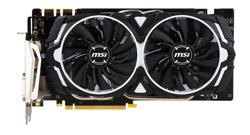
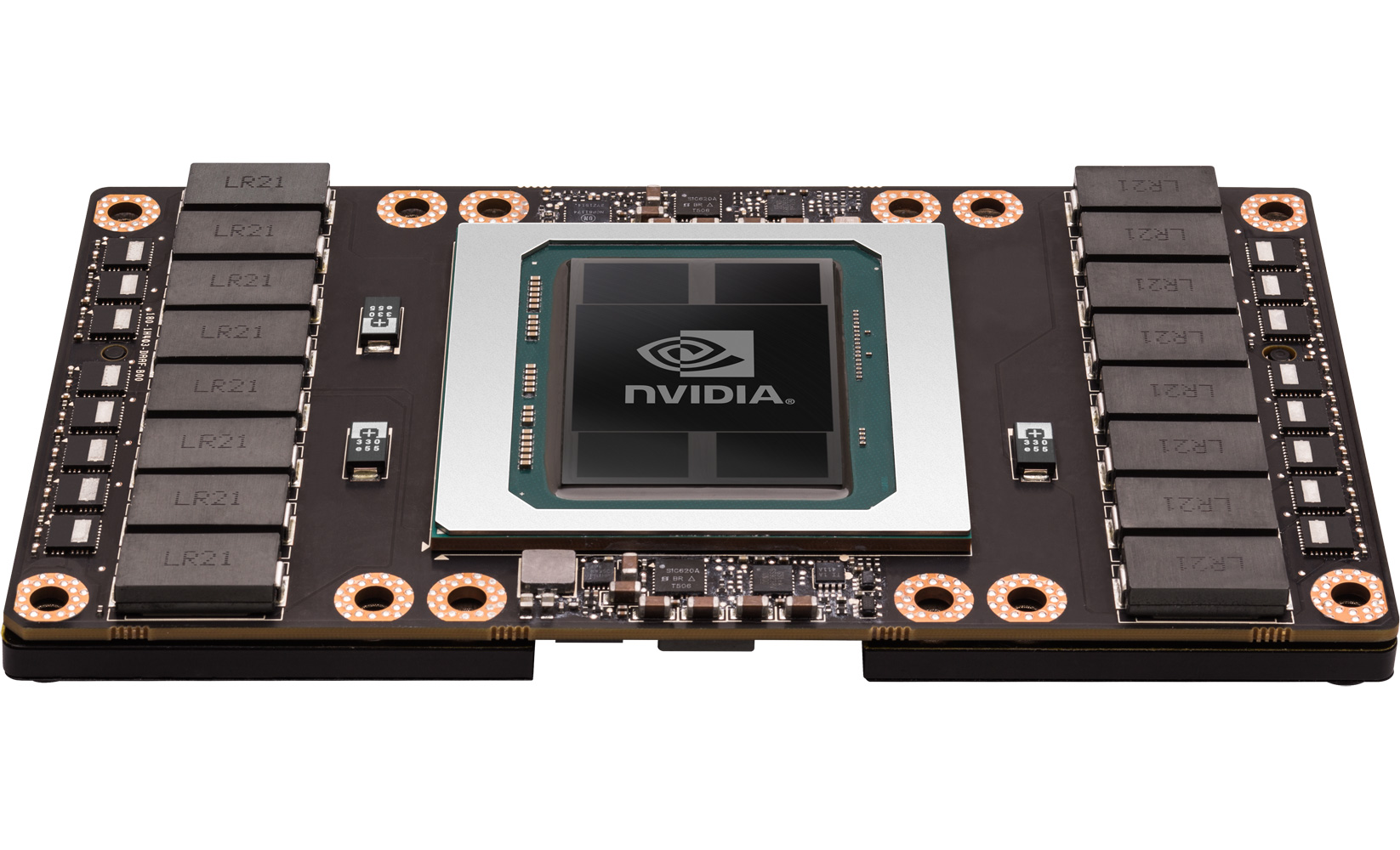
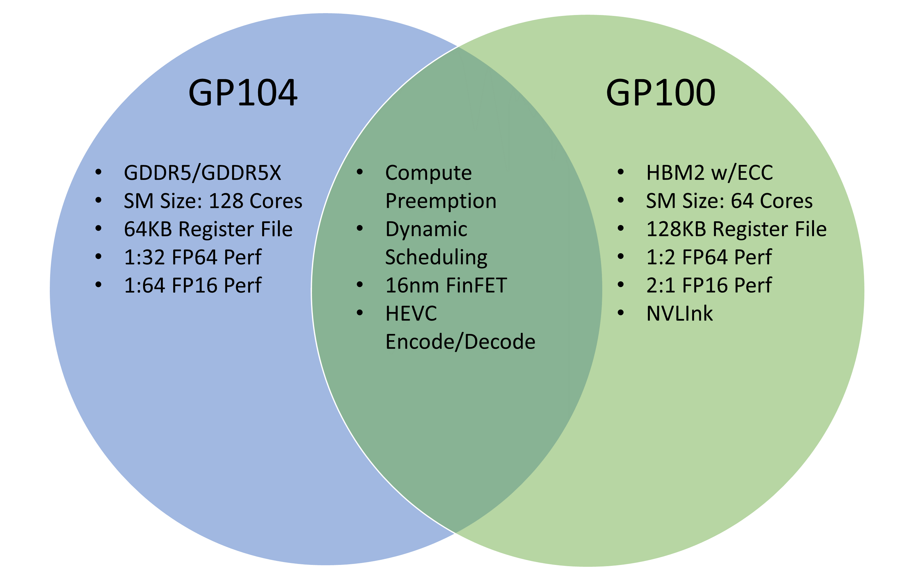
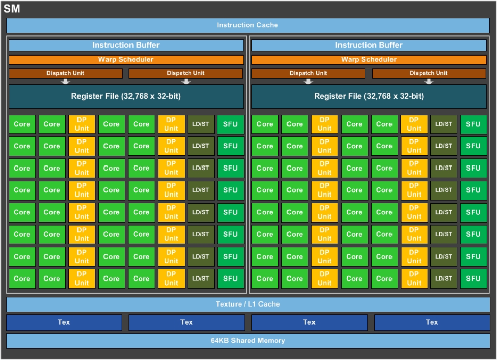
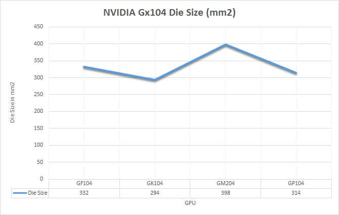
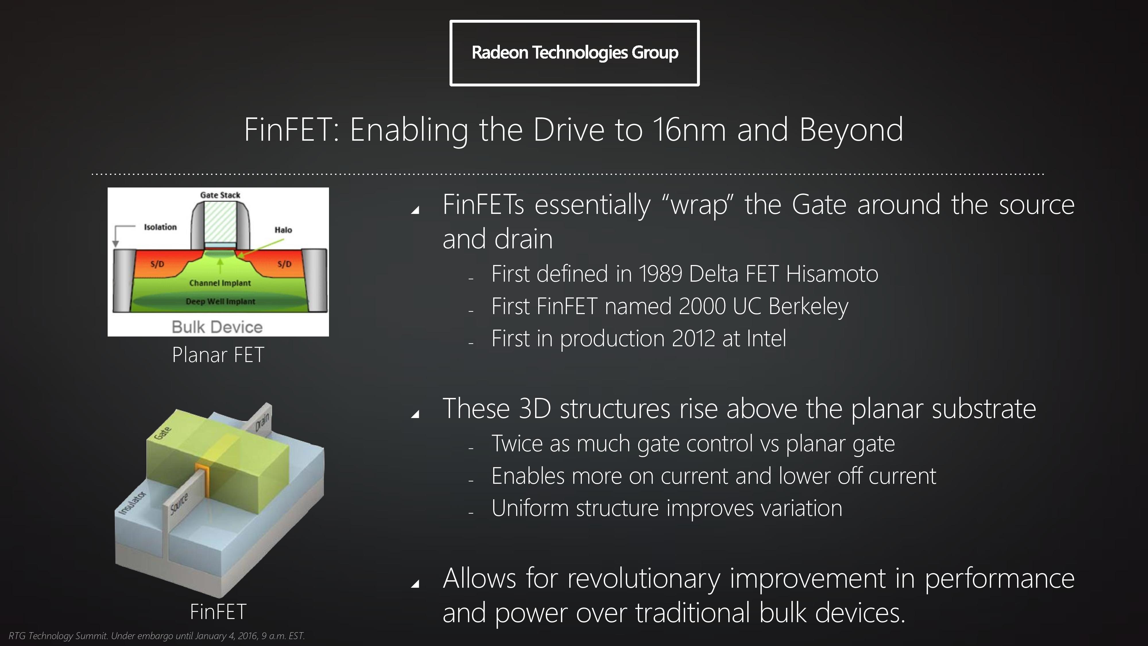
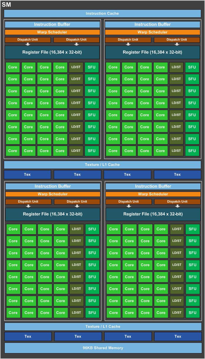
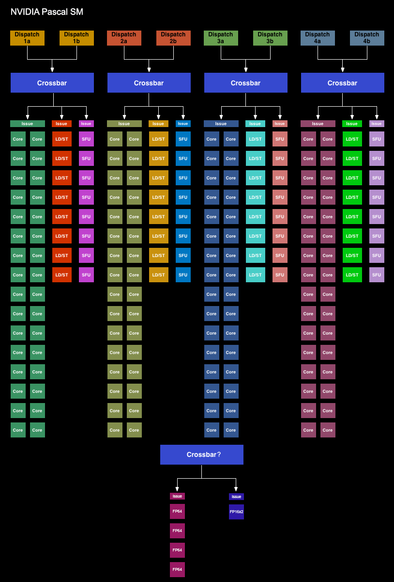
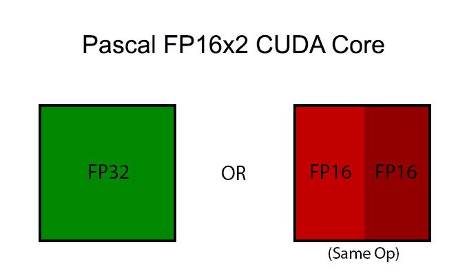
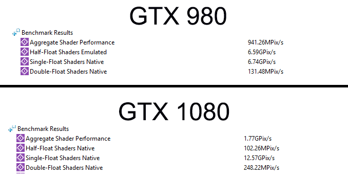
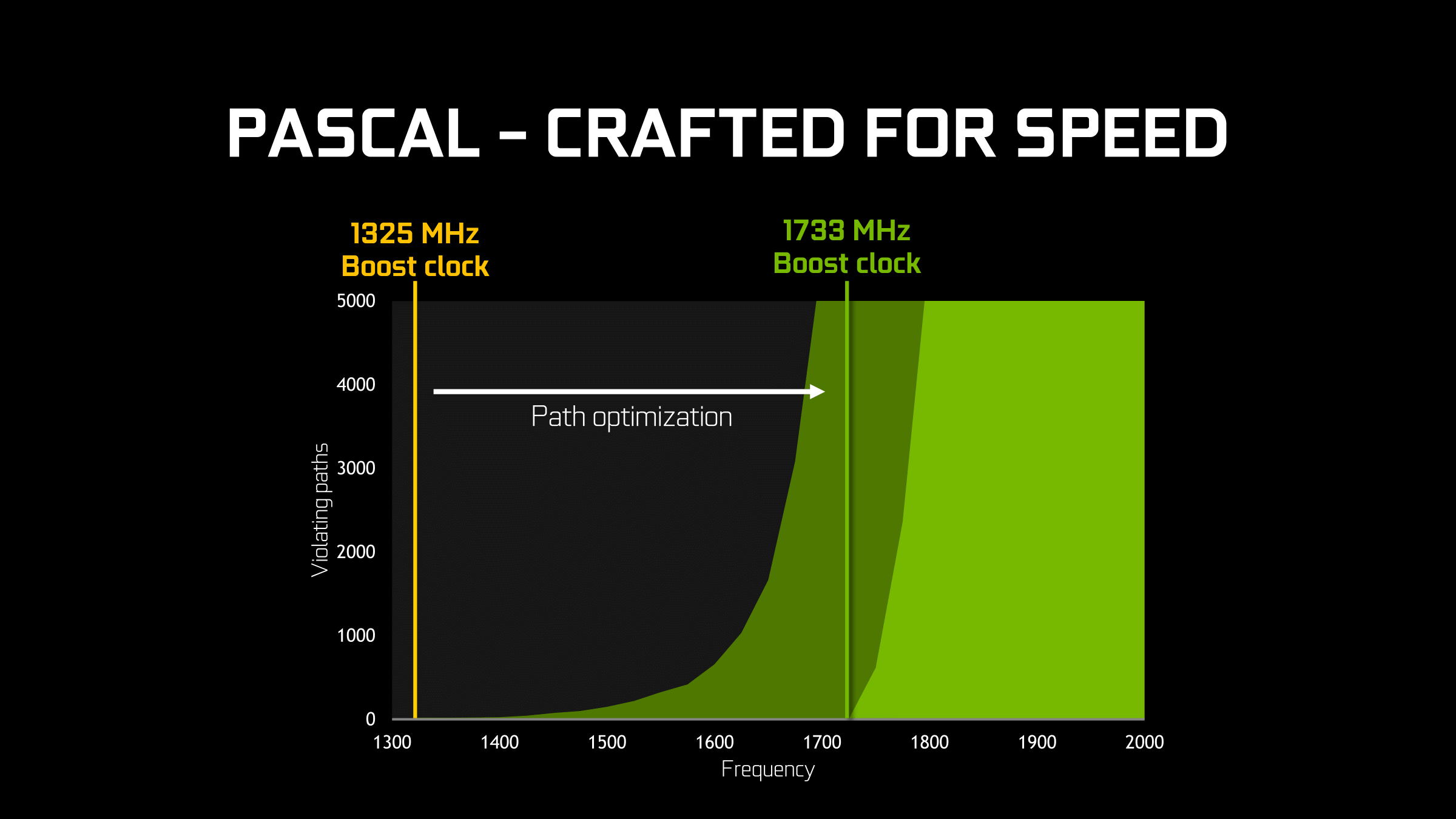
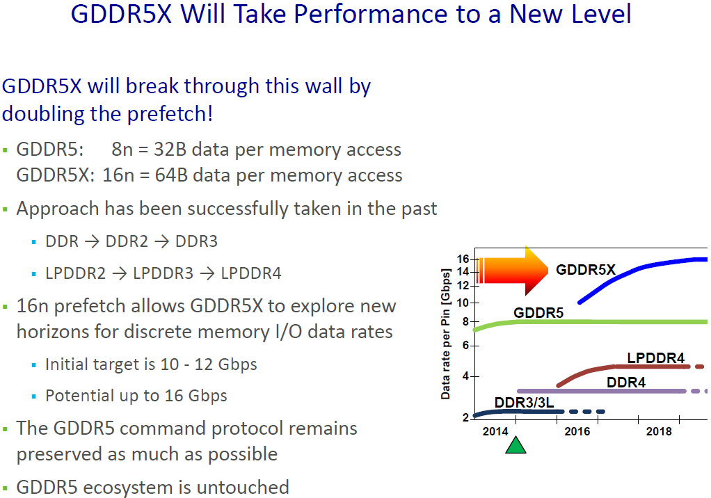
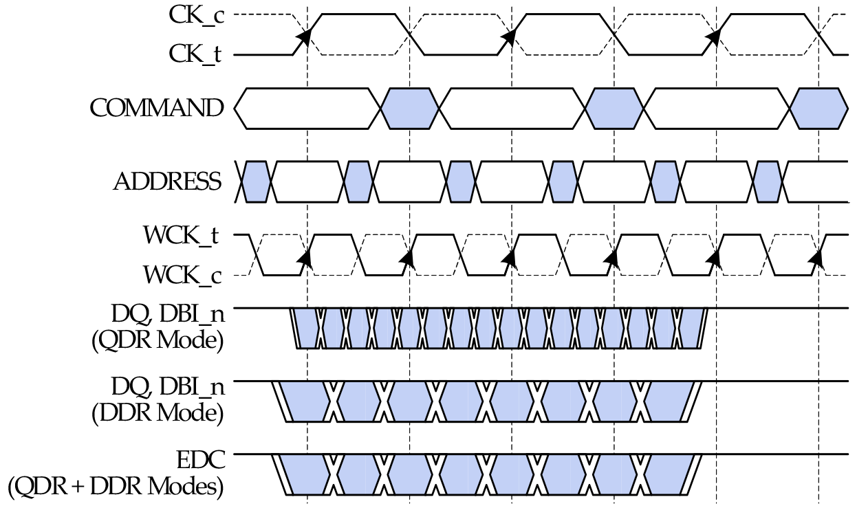
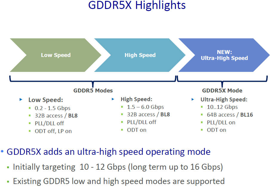
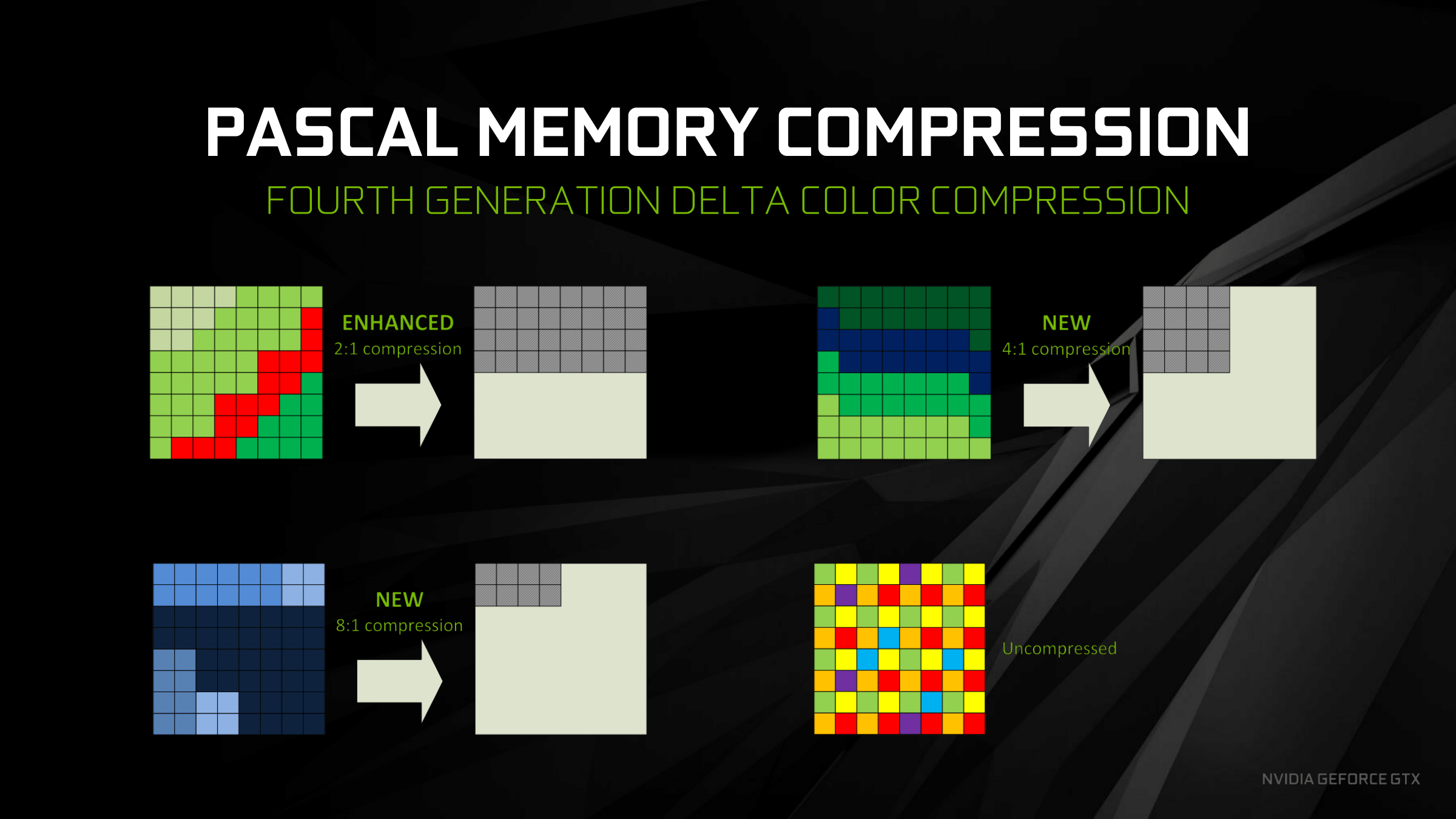
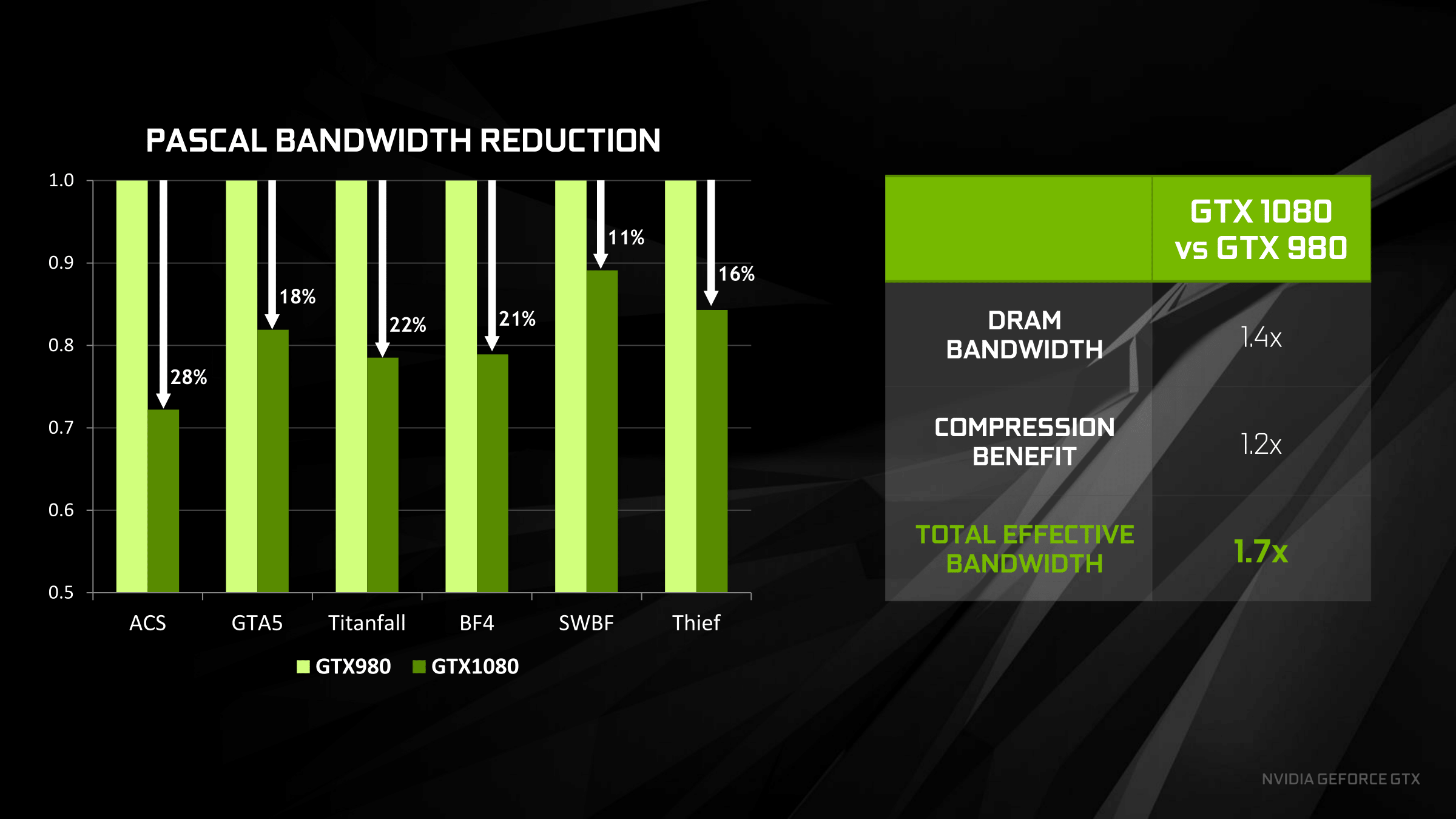
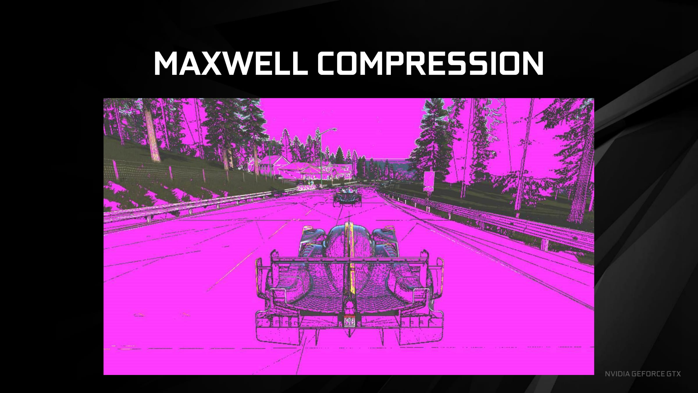
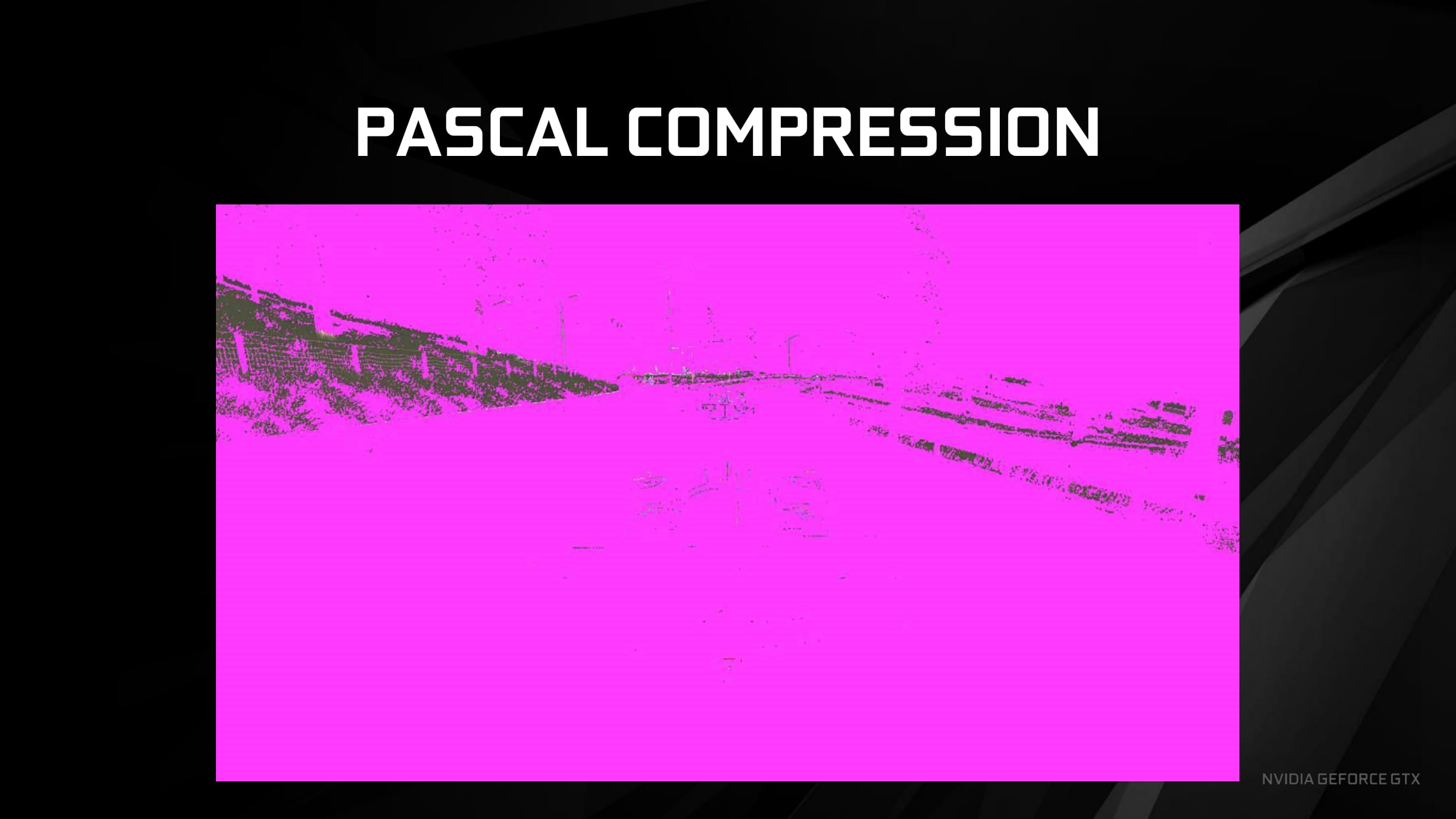
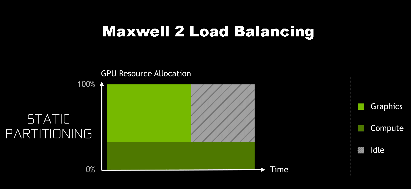
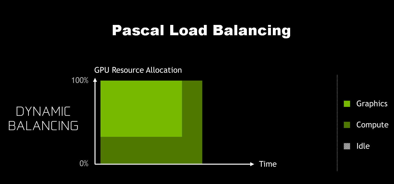
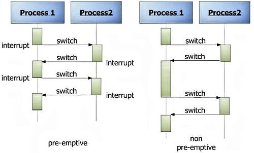
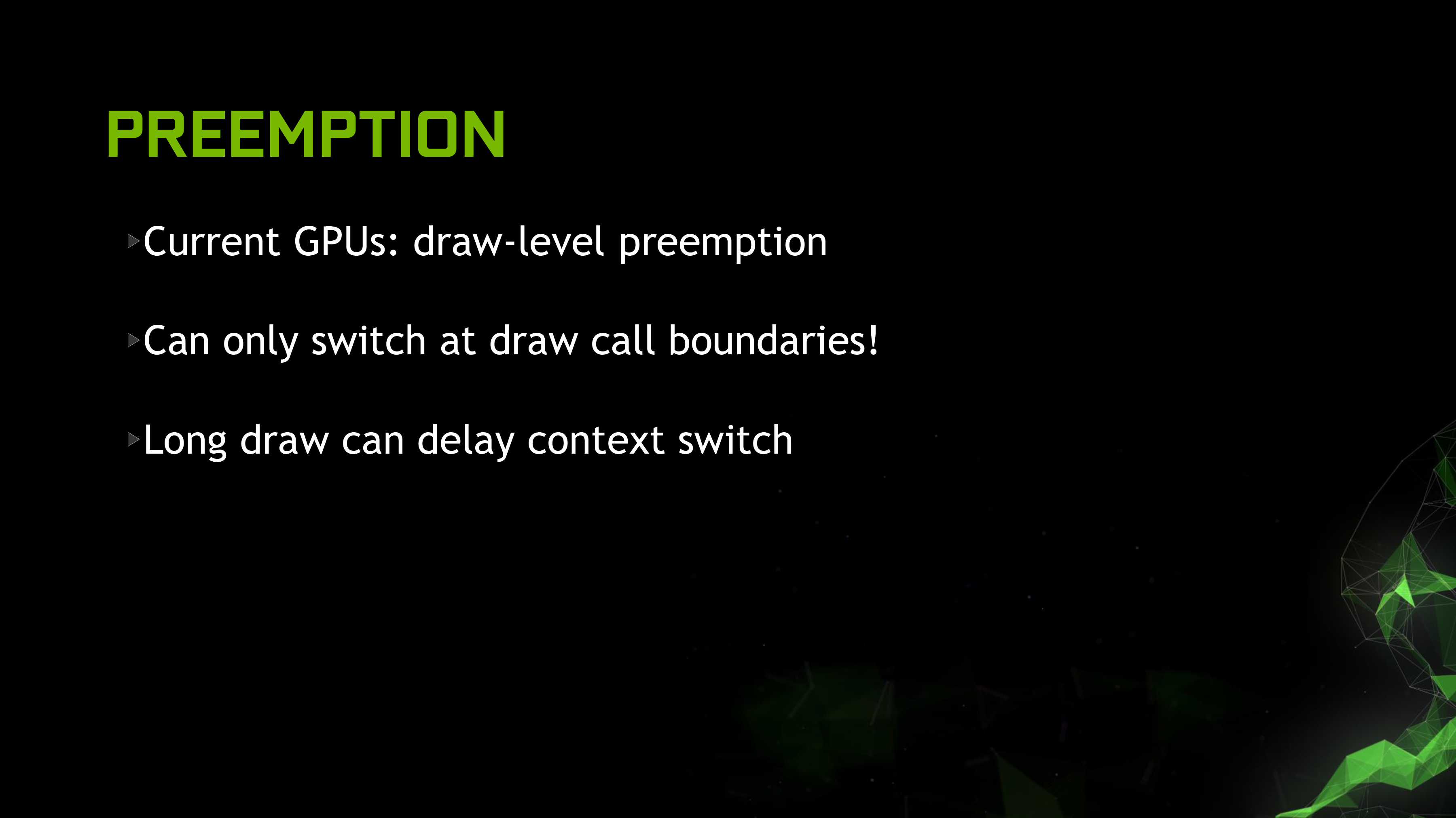
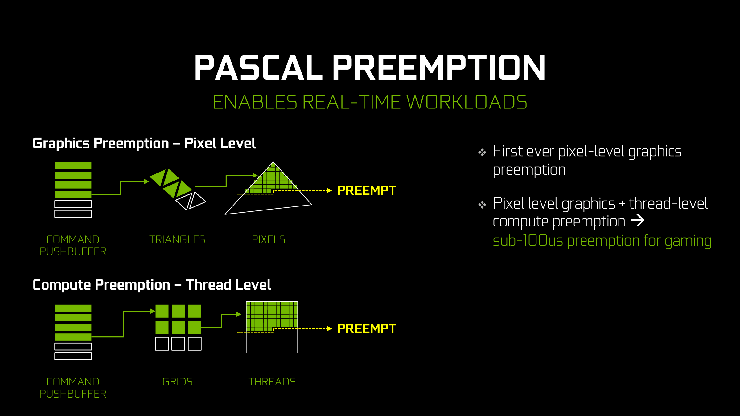
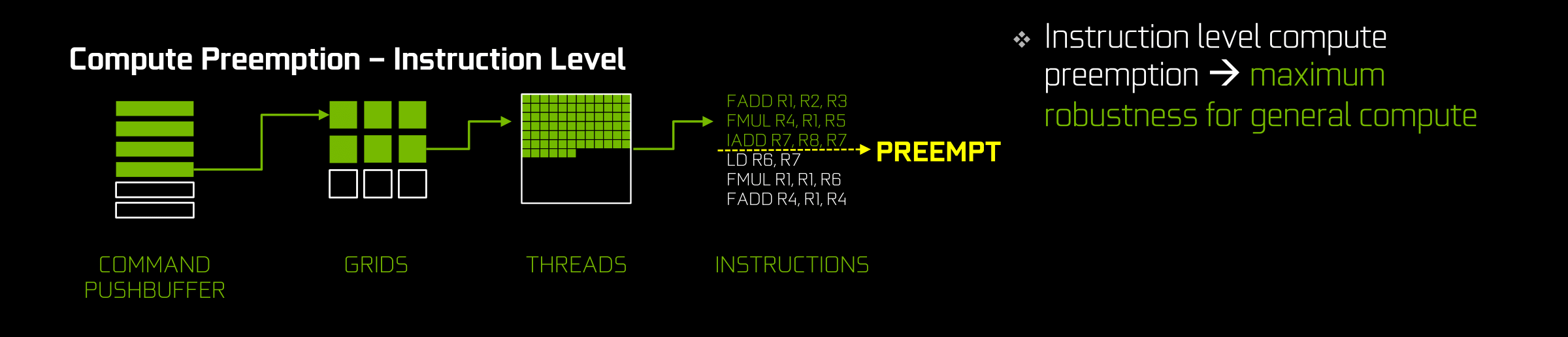
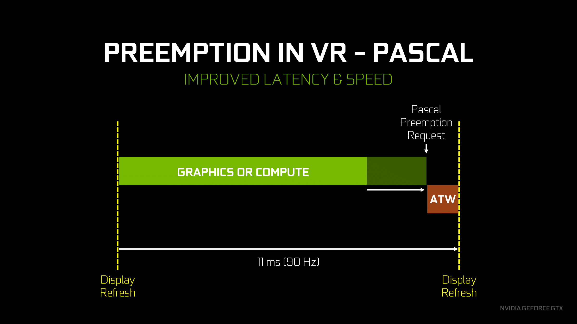
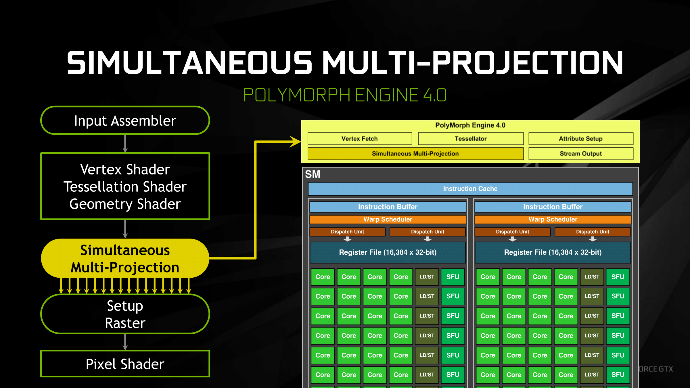
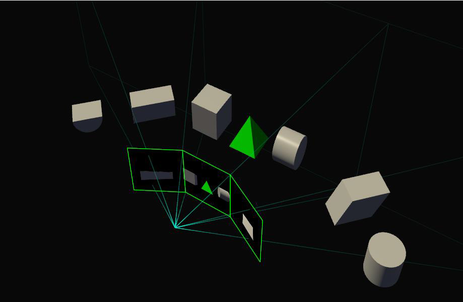
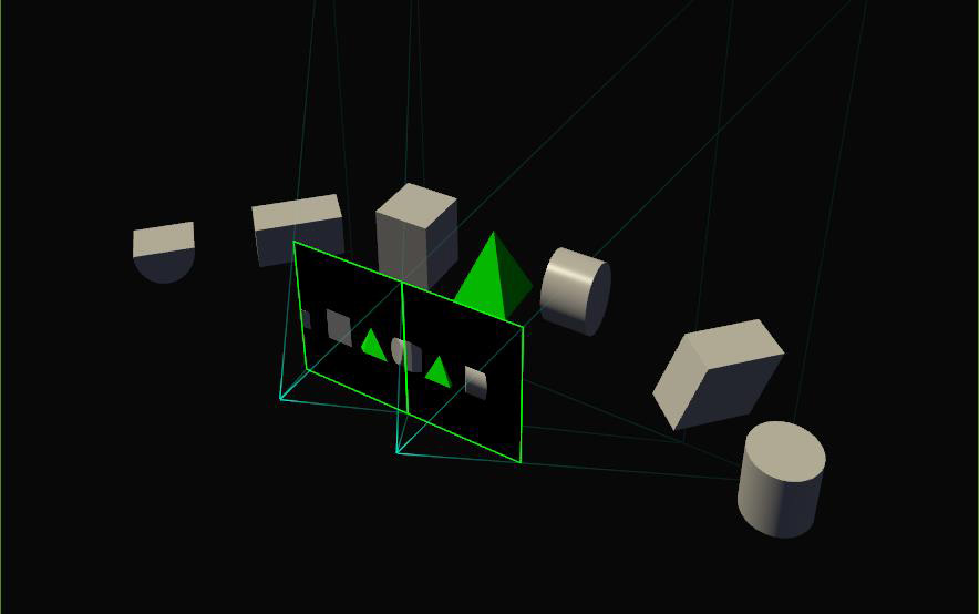
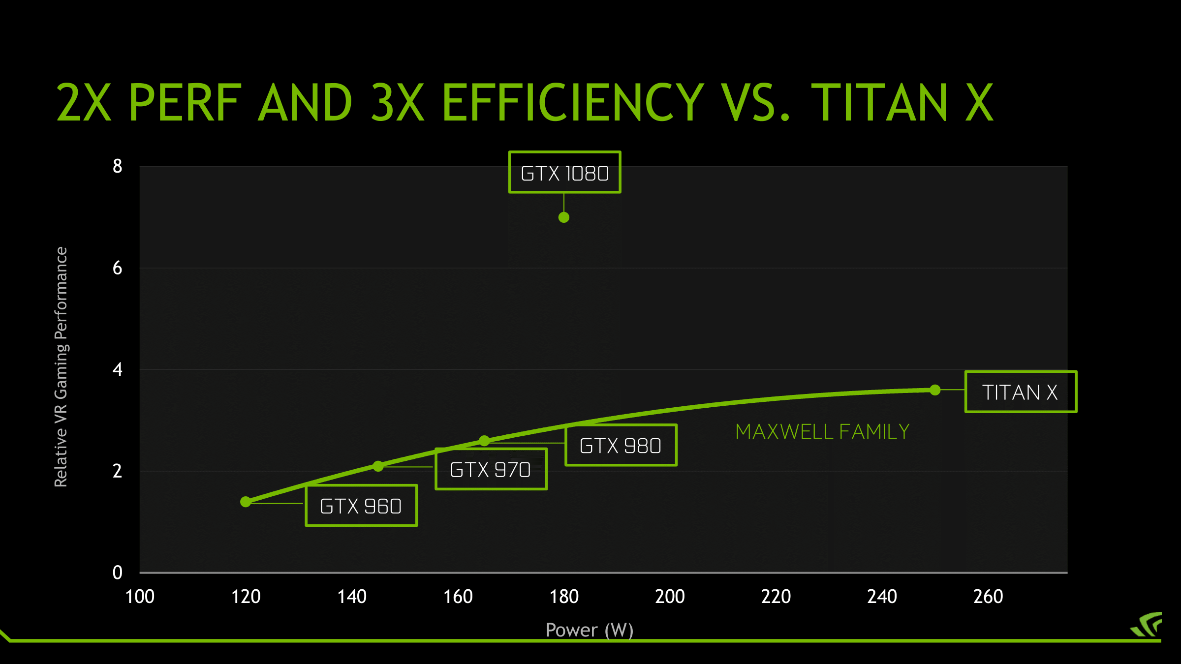
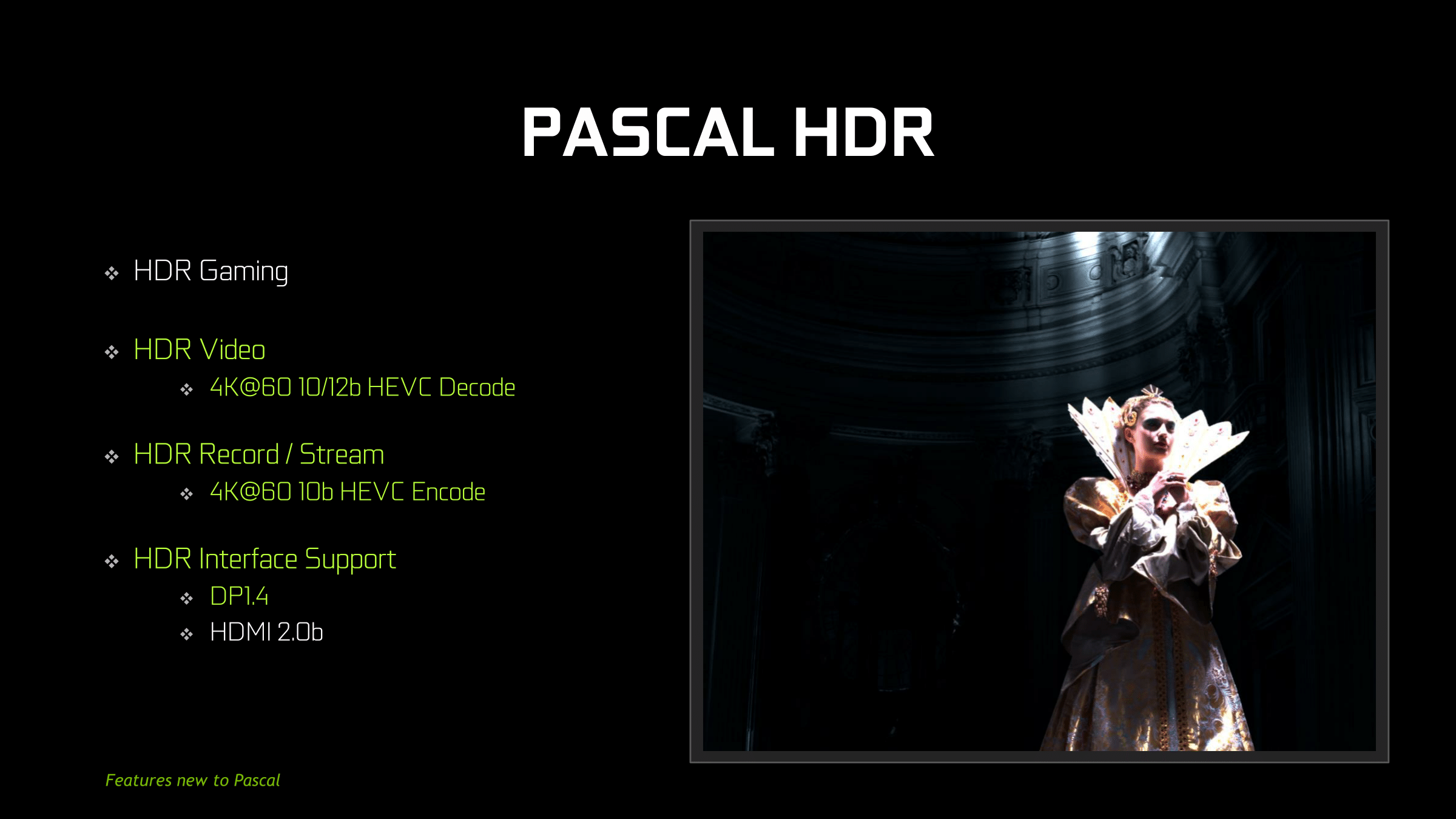
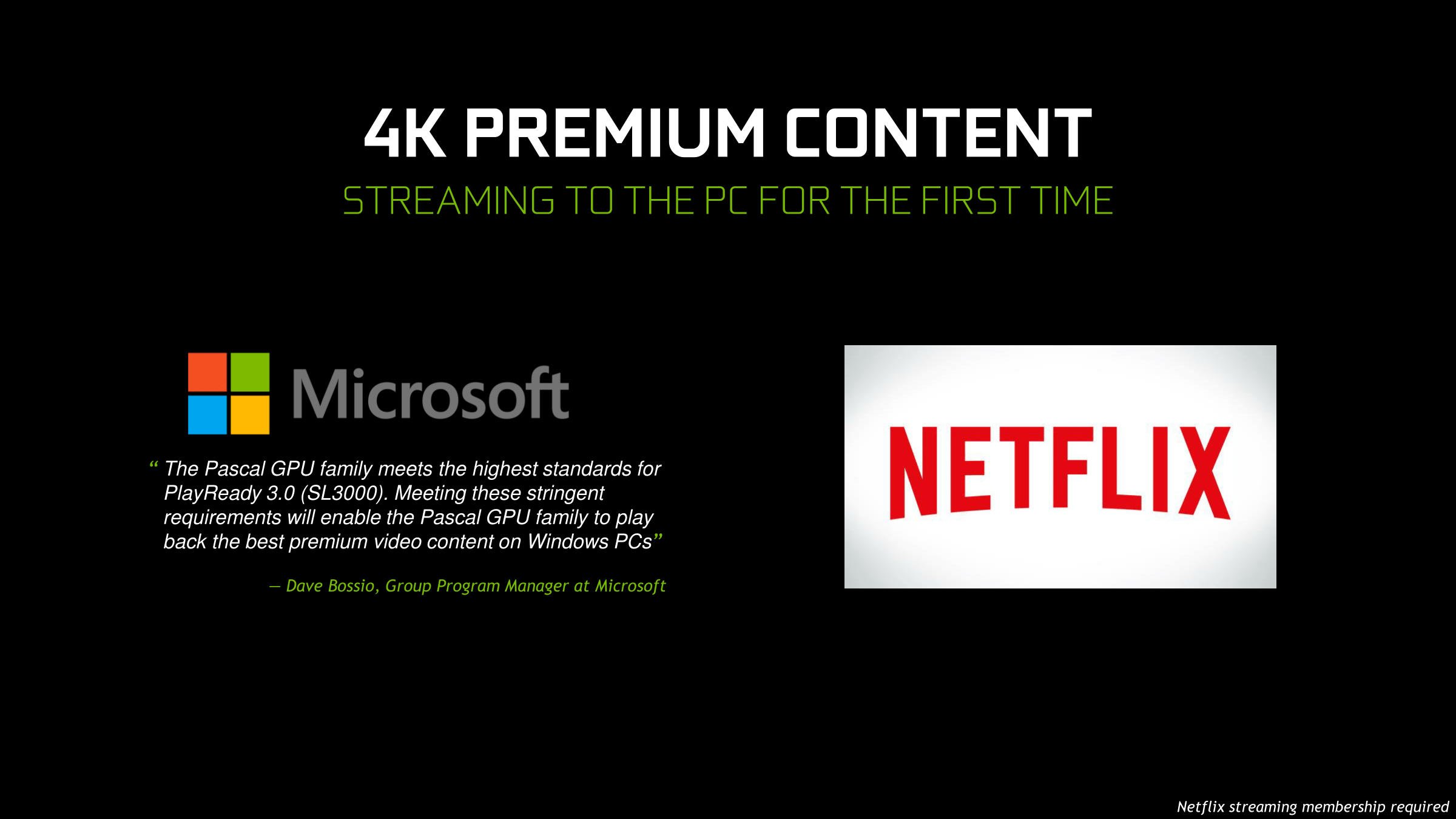
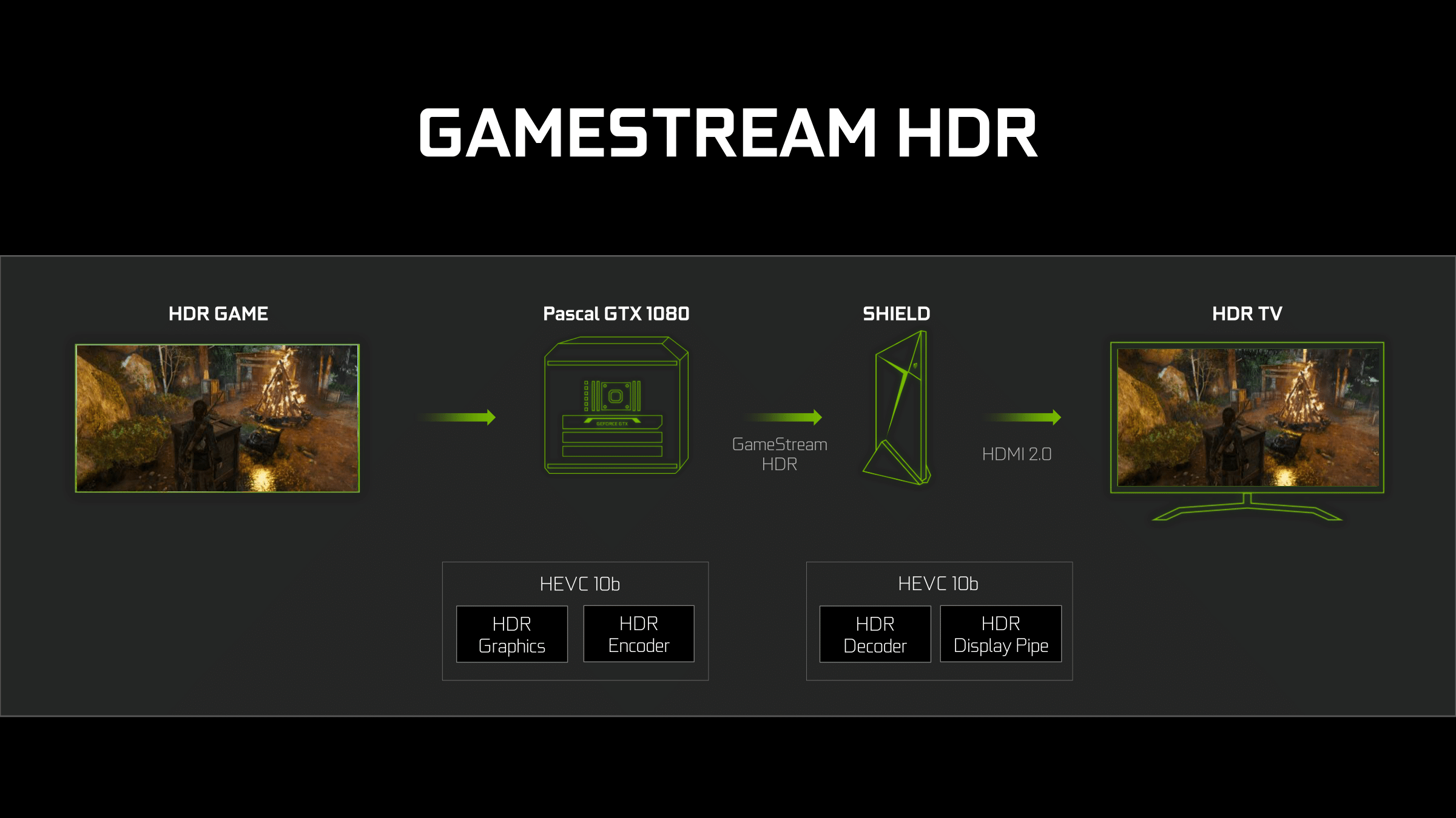
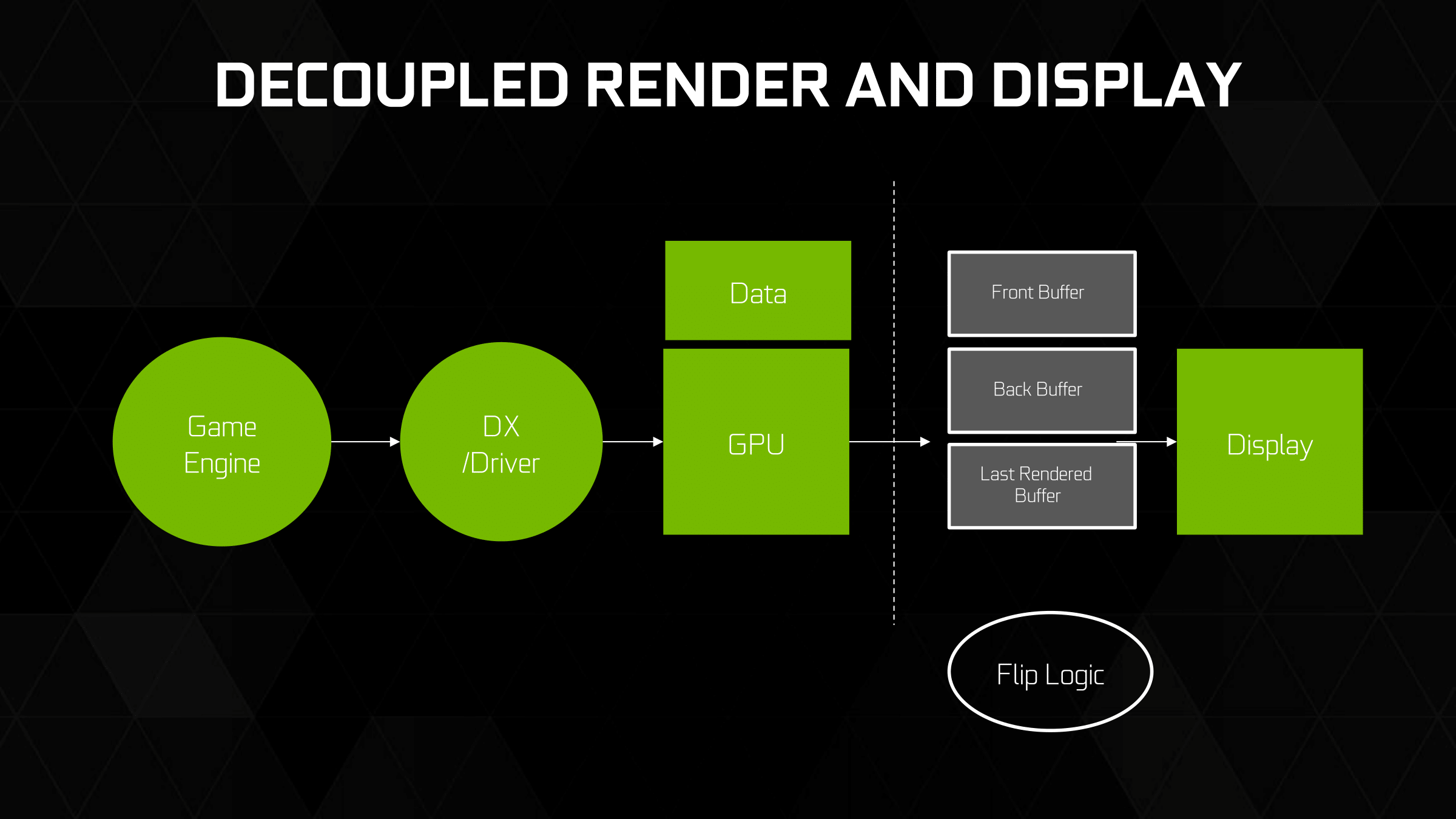
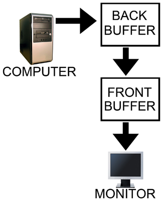
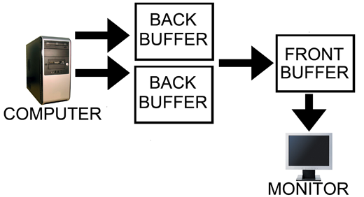
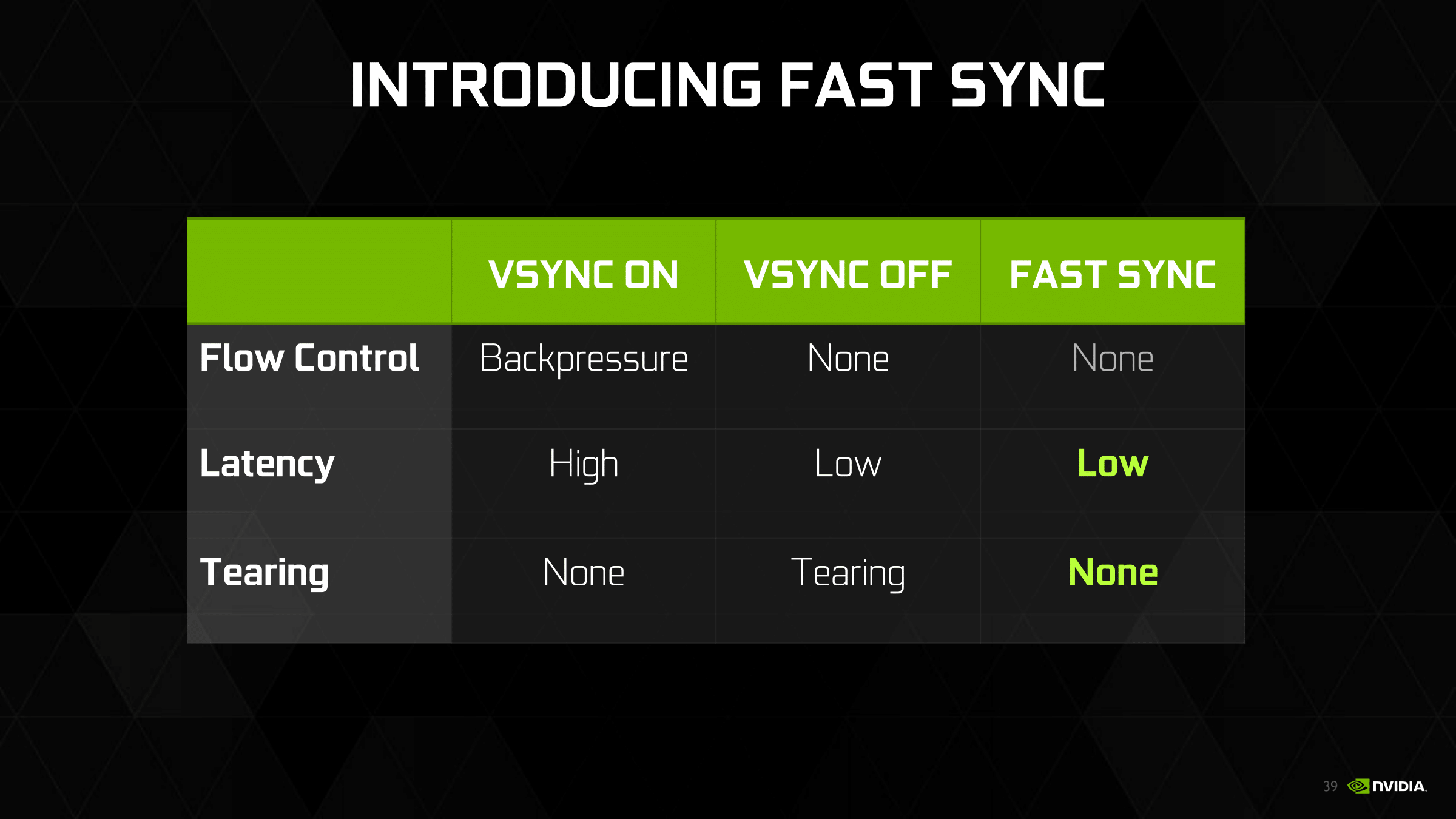
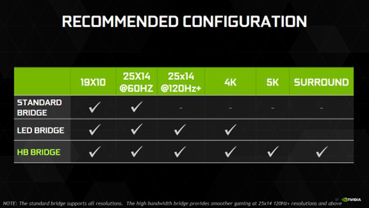
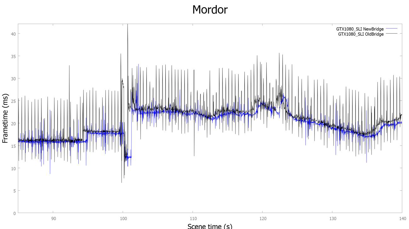
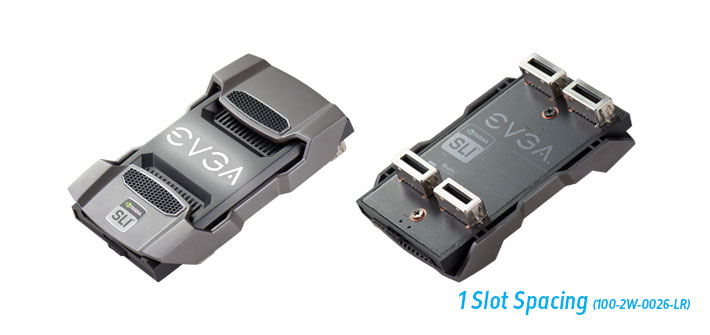
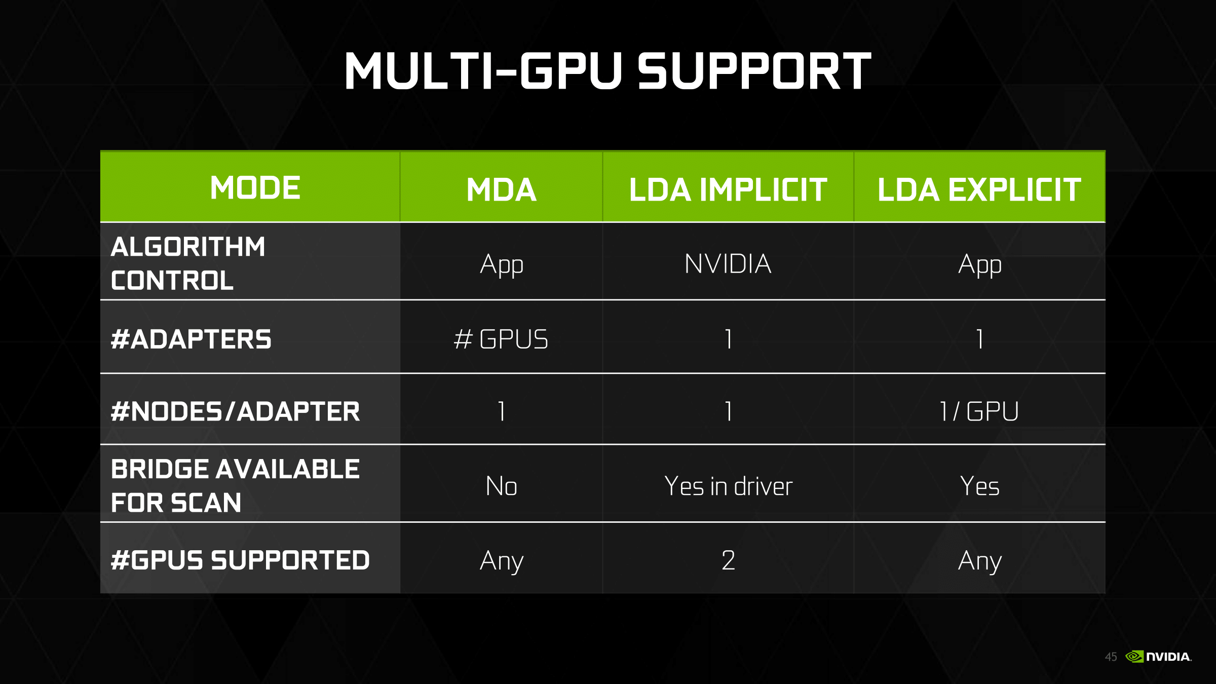
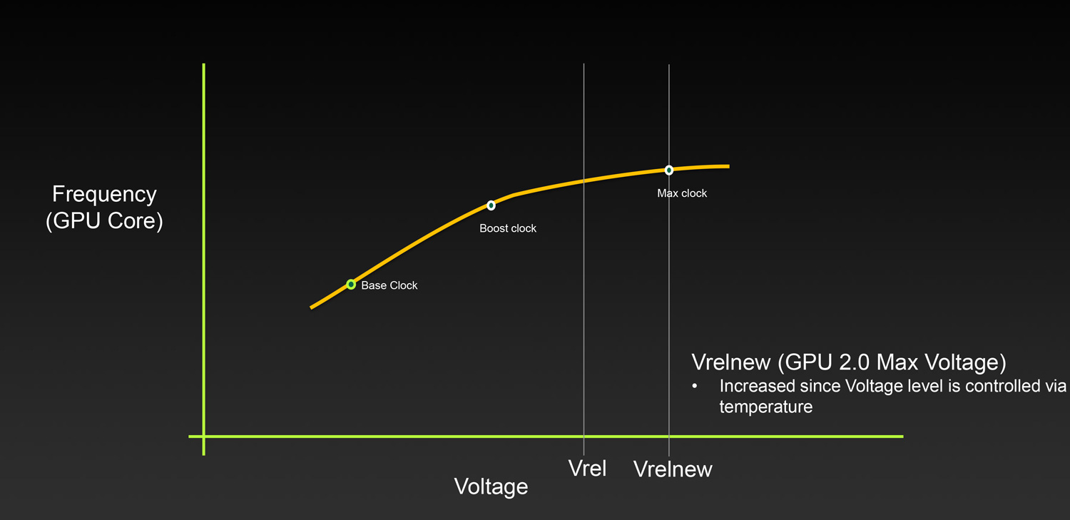
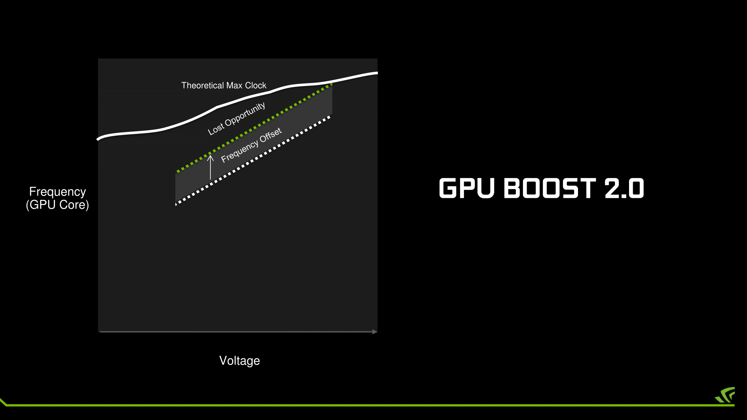
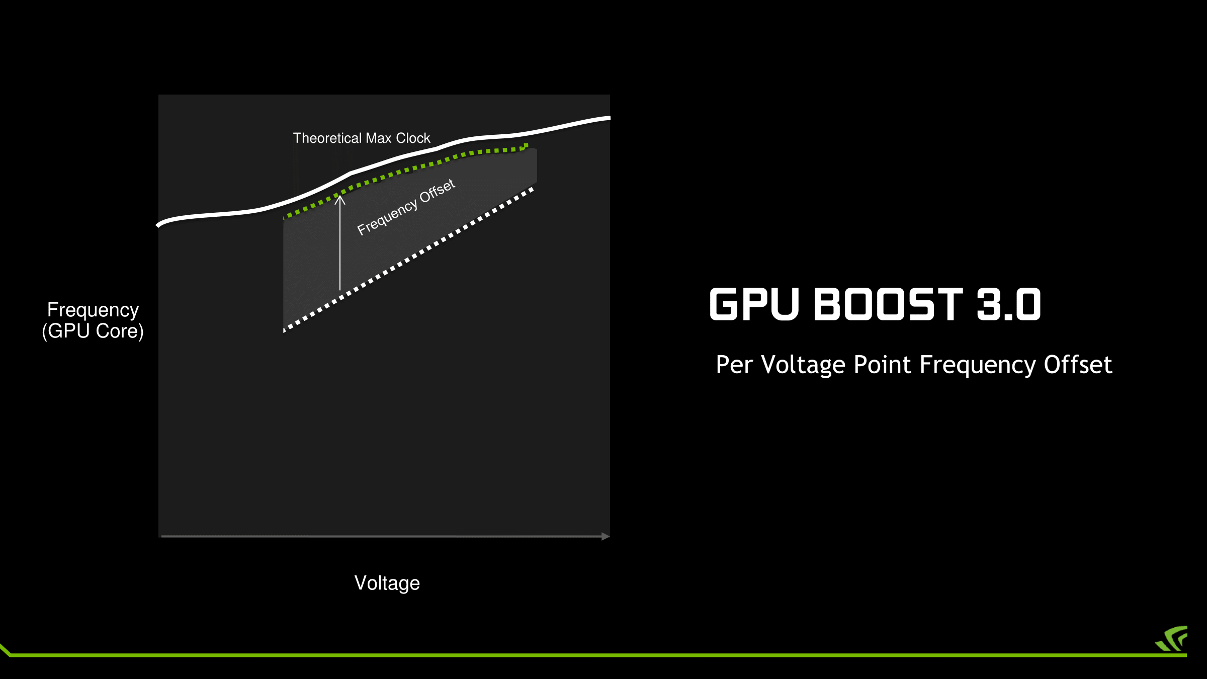
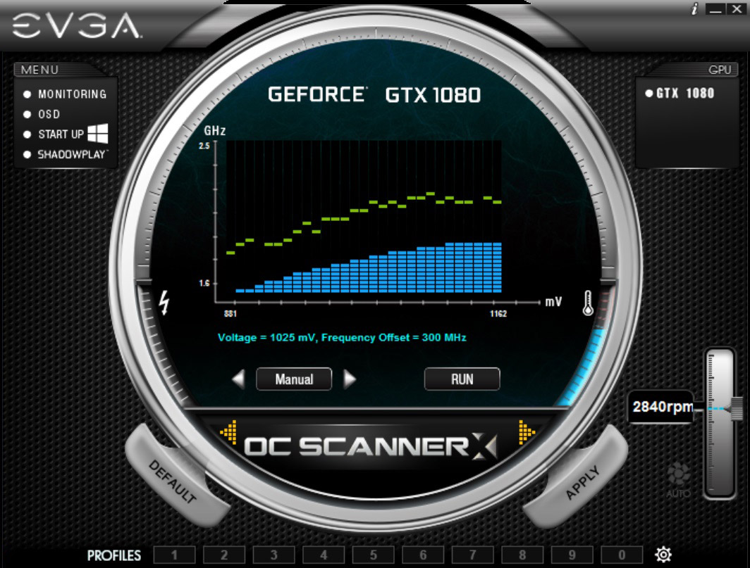
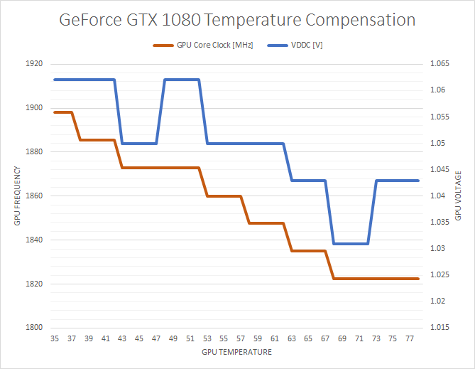
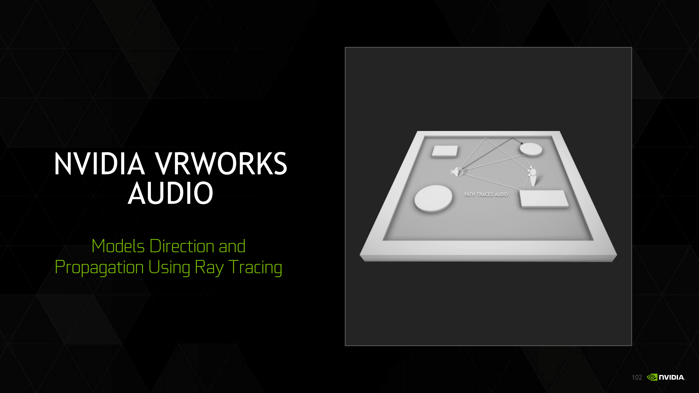
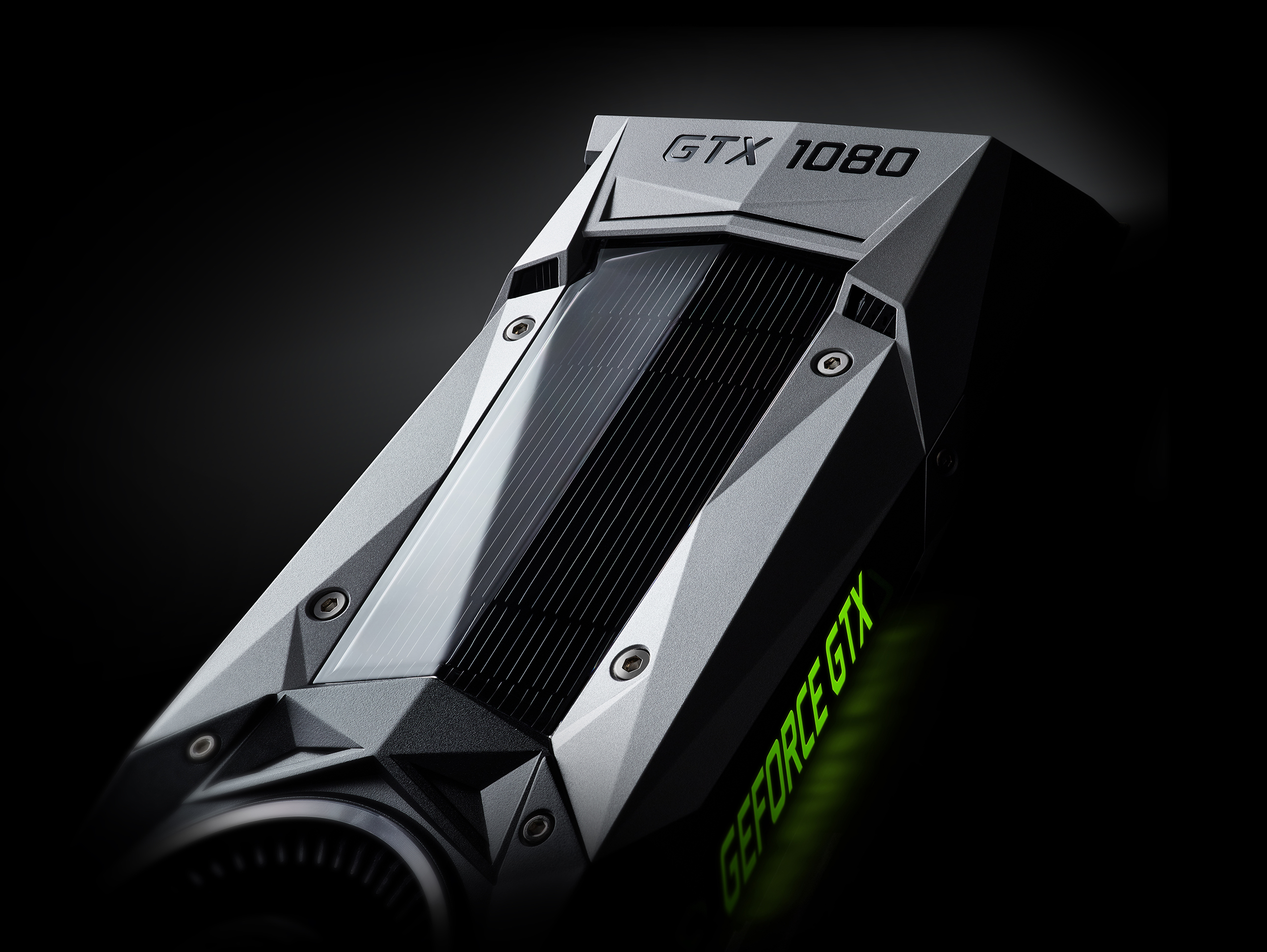
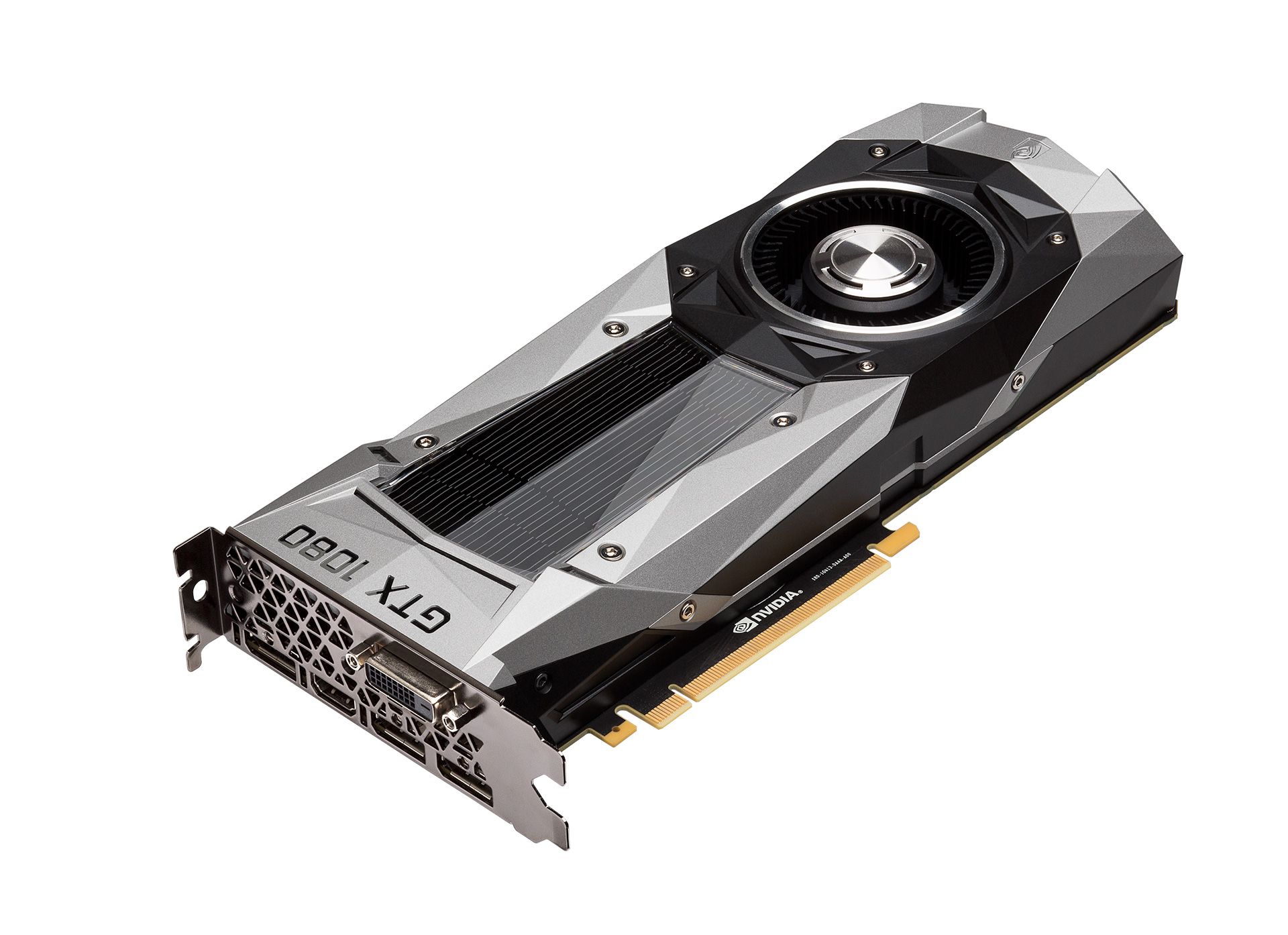
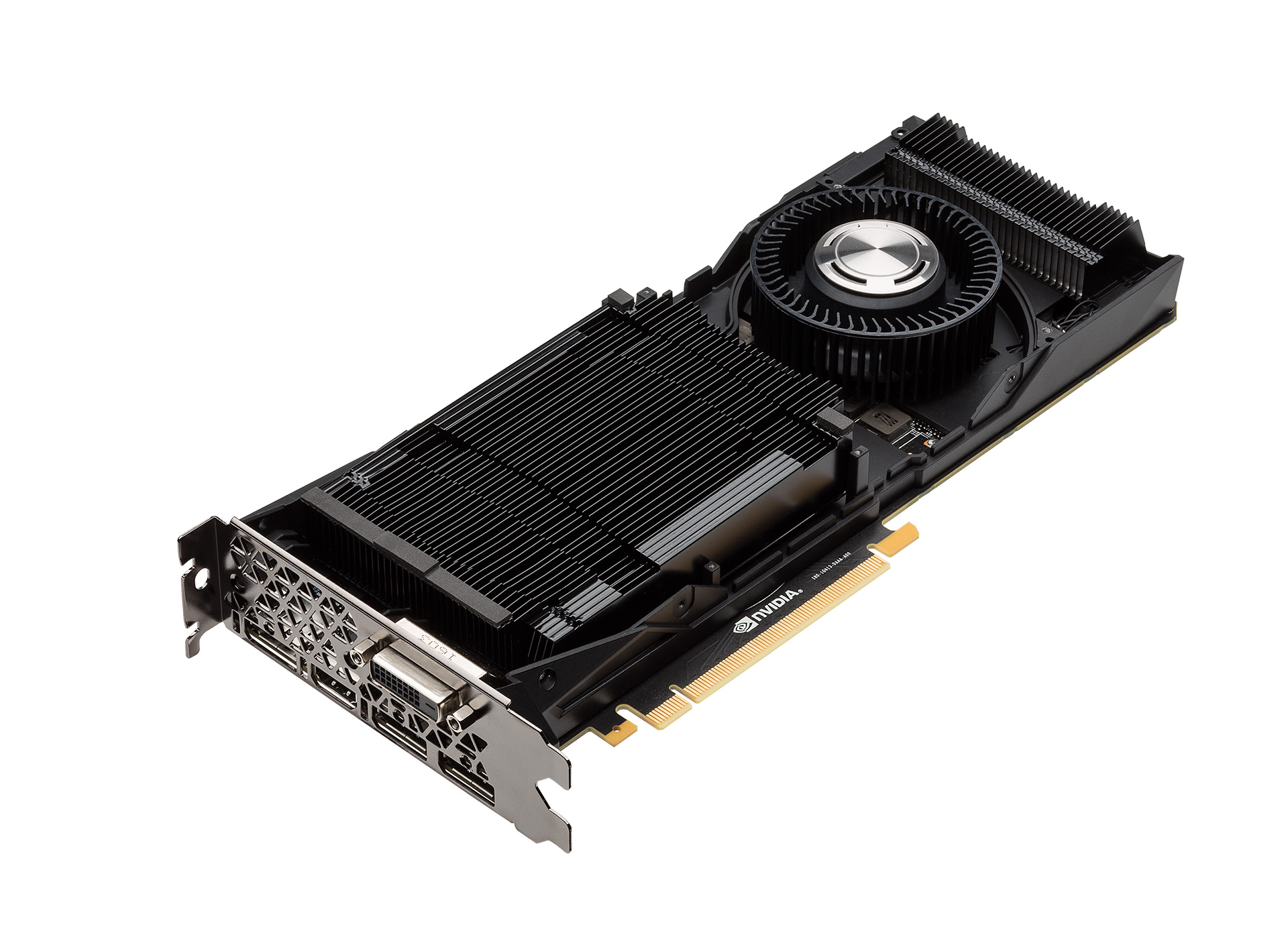
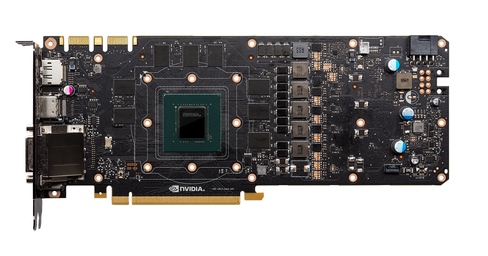
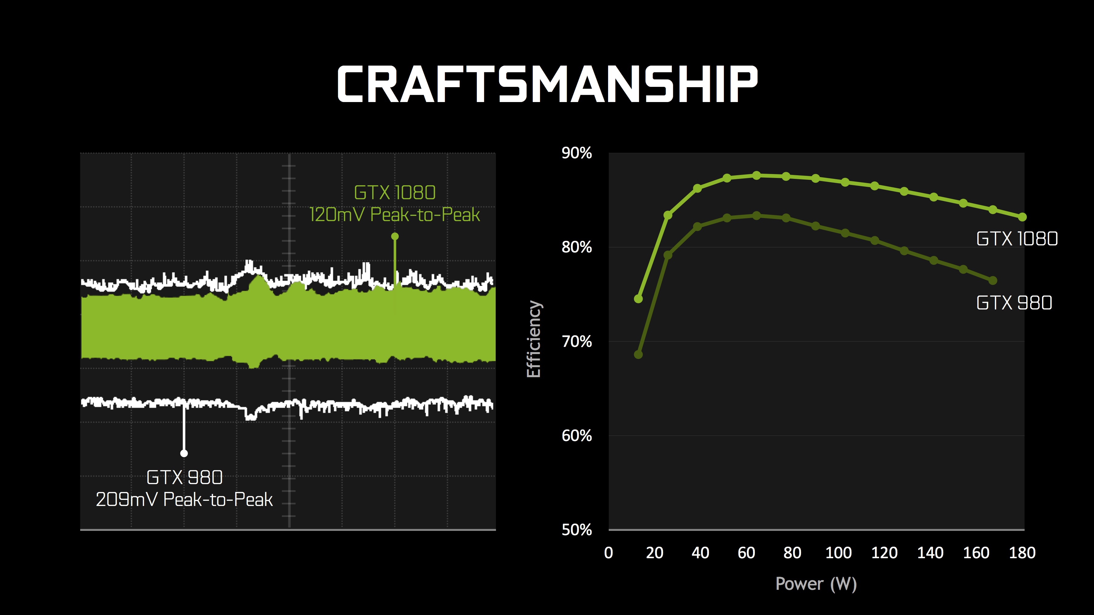
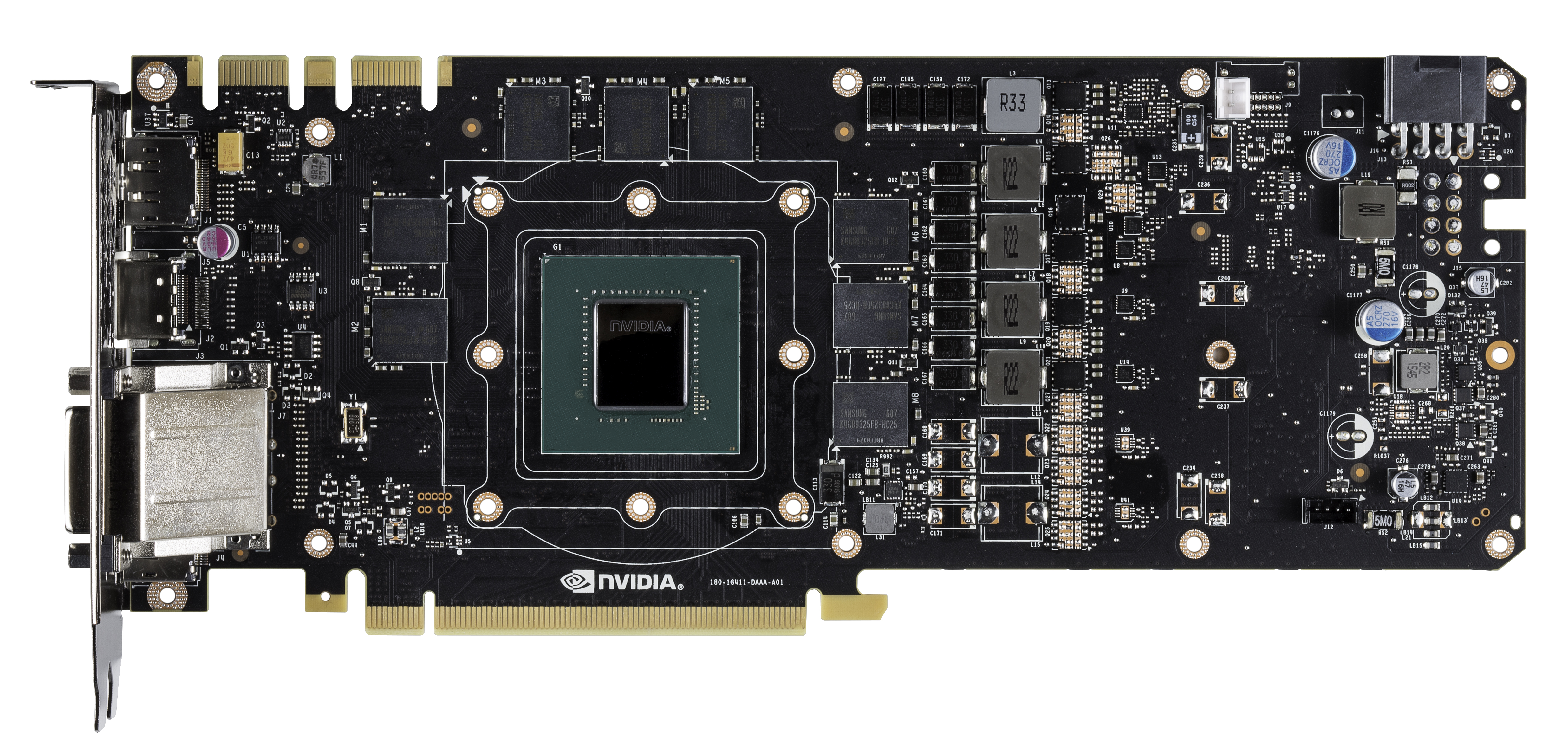
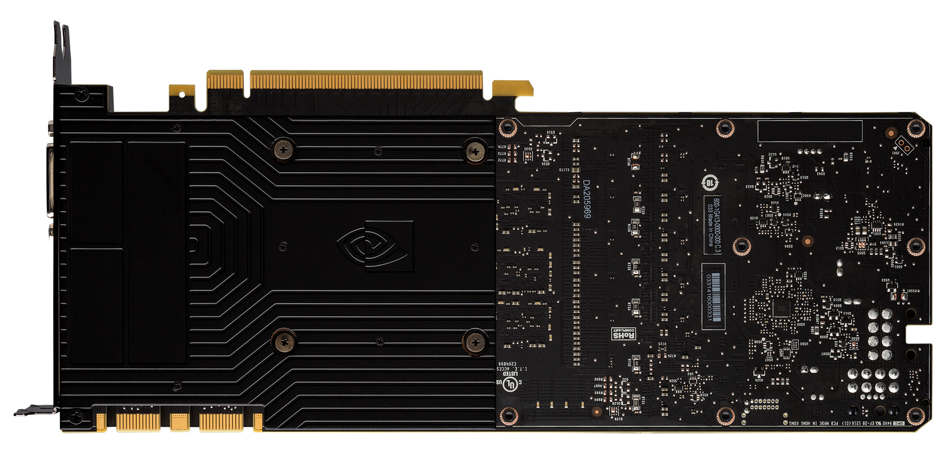
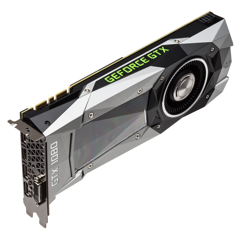
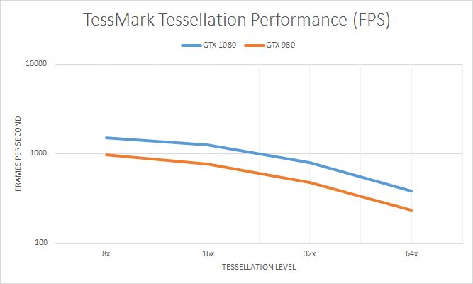
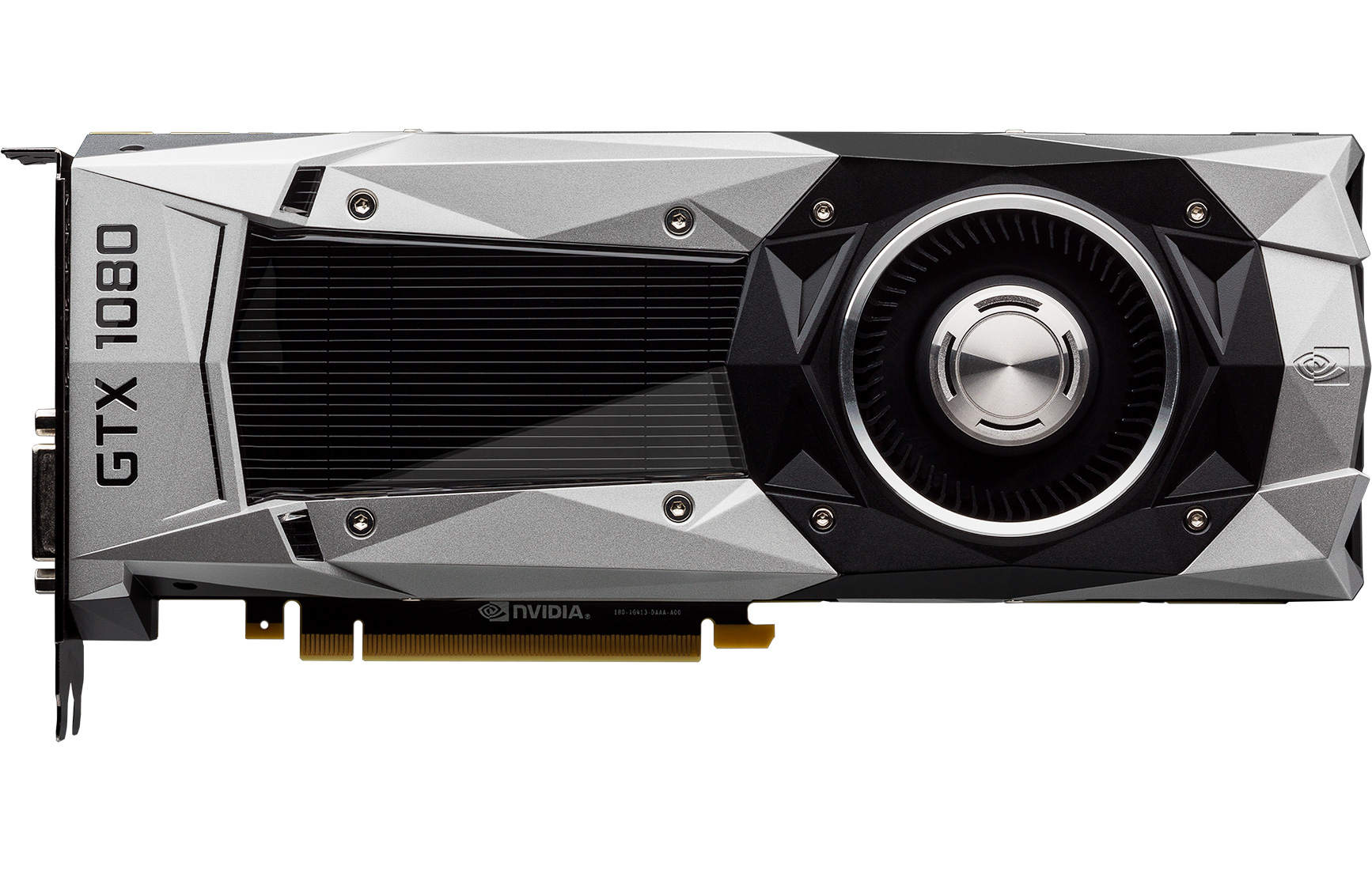
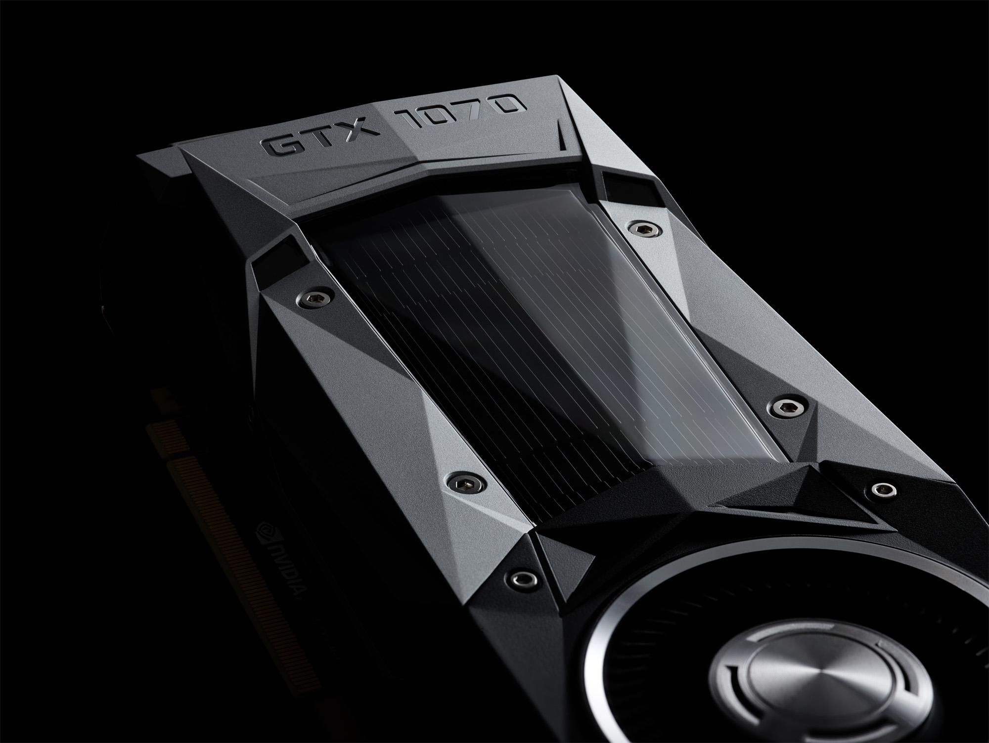