原文地址:https://fuse.wikichip.org/news/525/iedm-2017-isscc-2018-intels-10nm-switching-to-cobalt-interconnects/
原文作者:David Schor
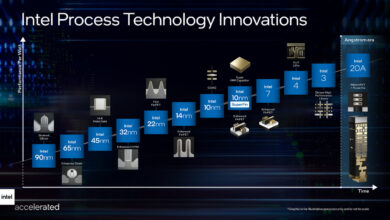
At the 2017 IEEE International Electron Devices Meeting (IEDM) in San Francisco, Intel formally detailed its 10-nanometer process technology. This leading-edge process is expected to be utilized by many of their future products, including their FPGAs and desktop and server microprocessors.
The 10 nm process was presented by Chris Auth, vice president at Intel Corporation and the director of advanced transistor development. Auth was responsible for leading the development of Intel’s 10 nanometer high-performance CMOS logic transistor process.
Because this article was planned for late January, we’ve decided to withhold publication and incorporate additional 10nm details from the 65th International Solid-State Circuits Conference (ISSCC) which was held earlier this week. At ISSCC, Zheng Guo presented Intel’s 10nm SRAM devices which are discussed later in this article.
Overview
The major features are:
- 2.7x density over their 14nm
- 3rd generation FinFET transistors
- Self-Aligned Quad-Patterning (SAQP)
- Contact-over-active-gate (COAG)
- Cobalt local interconnect, vias, and trench contacts
- Cobalt interconnect liners
Design Features
Intel’s 10 nanometer largely builds on many of their existing technologies.
- 2nd generation Low-κ spacer
- 3rd generation of fully depleted FinFET transistors
- 5th generation High-κ metal gate
- 7th generation strain silicon
- Self-Aligned Quad Patterning (SAQP) for the critical patterning layers (3 critical layers)
- 4 workfunction metals on the base process
- Self-Aligned trench contact
They first introduced their fully-depleted FinFET structures at the 22 nm node and most recently in their 14 nm node. Likewise, the High-κ gate was first introduced in their 45 nm node and have been used ever since. It’s worth pointing out that in addition to the 4 workfunction metals used for the base process, Intel noted that they also have 6 workfunction metals that can be introduced for high-Vth transistors when needed.
Beyond Conventional Scaling
While the time between each consecutive technology nodes have lengthened, Intel has attempted to compensate for this by accelerating the density of each process. Going from the 22-nanometer node down to the 14-nanometer, transistor density increased by 2.5x. Likewise, going from the 14-nanometer down to the 10-nanometer node we see a 2.7x increase in density. In other words, from the introduction of the 22 nm node in late 2011 to the ramp-up of Intel’s 10 nm in 2018 we have observed close to 7x density increase over the span of 7 years.

Key Dimensions
The key transistor dimensions for Intel’s 10nm are:

For their 10nm paper, Intel used a 46 nm fin height transistor (although that’s discussed further later on) with a pitch of 7nm and a gate length of 18nm. This roughly translate to around 100nm gate width. Below is a rough diagram of the features:

WikiChip’s Transistor Diagram (simplified)
In order to enable a pitch down to 34 nanometers, such as in the case of the fin pitch and the minimum metal layer, Intel has moved to self-aligned quadruple patterning (SAQP). Dual patterning (SADP) was first introduced at the 22nm node and is continued to be used for the down to the 44nm pitch. For the wider pitch, single patterning is used.

At 272nm cell height and 34nm fin pitch, there are eight lines that can be used. It’s worth noting that Intel uses different cells for different applications.
Back-End
Intel 10nm process consists of a 13-layer metallization stack.

For the critical dimensions which is 34 nm fins and the two metal layers, Intel uses quad patterning which adds four steps to the flow ? deposition on the spacers followed by the etching steps. Metals 2 through 5 as well as the gate patterning get away with just double patterning.
Going Cobalt
As you shrink the transistor geometry you need to shrink the wires as well for the chip to benefit from the higher density. Scaling the wires has been an increasingly complicated task. While the solutions are incredibly complex, the fundamental problem is simple ? the longer and narrower the wires get, the higher the electrical resistance is.

Using the incredibly over-simplified interconnect structure above for RC analysis, the resistance of the wire can be described as R = ρ ? [L / (W ? H)] where ρ is electrical resistivity of the interconnect, L is the length of the wire, and (W * H) is the cross-sectional area.
Exactly 20 years ago, at IEDM 1997, Daniel Edelstein, an IBM Fellow, presented their paper announcing their plan to insert a Cu BEOL technology into production. IBM ramped up their 180nm process (CMOS-8S3) in 1998 which was later used for the POWER4 chips. At the 180nm process IBM replaced the Aluminum interconnect with copper for its significantly lower resistivity, higher scalability, and higher current density capabilities.

20 years and 10 technology nodes later, we’re finally see copper running out of steam. At IEDM Intel made a surprise announcement with 10nm using cobalt interconnect for the first time in high-volume manufacturing. There’s just one interesting fact: cobalt doesn’t actually have lower resistivity compared to copper.

Note that since bulk Cobalt is hexagonal, there are two values depending on the transport (perpendicular and parallel axis).
From the table above it can be seen that copper has considerably lower resistivity than aluminum, tungsten, and cobalt. So why switch? Electromigration. The high-speed electrons that flow through the wire occasionally bump into the copper ions causing a momentum transfer, gradually skewing them in a certain direction. Using a pipe analogy, the metal density at one end decreases and piles up on the other end. The decreased density, or void, affects the reliability of the integrated circuit which eventually results in a failure due to the increased resistance.
To mitigate the problem and protect the wires, manufacturers introduced diffusion barriers and liners using other materials such as silicon/tantalum nitride and oxynitride. The barrier is used to to prevent metal diffusion into the dielectric while the liner is used as “glue” for the barrier and the copper. Once those are in place, the copper seed layer (metal plating) and then the bulk copper is added.

WikiChip’s simplified diagram of the interconnect.
This worked nicely, but there is a problem. As interconnect continued to shrink, the thickness of the high-resistivity liner/barrier for the copper interconnects stayed more or less the same. This is largely due to the difficulty in thinning it any further than the few nanometers it already is. This means that as the wires scale, the barrier itself takes up a larger and larger portion of the interconnect cross-sectional area. With the high-resistivity barriers slowly making up a larger portion of interconnect, it begins to dominate the resistivity of the wire itself.

This isn’t the only issue affecting the wire scaling. The mean free path is the average distance the electron travels between collisions. Since the mean free path λ for copper is almost 40nm, then as the copper interconnect approach λ or 40nm, the copper electrons will begin to scatter far more often from the various surfaces and grain boundaries because they are so area-constrained. This excess scattering increases the resistivity of copper.

So while the transistor performance has been improving, the copper wire resistance has actually been increasing as the wire got smaller. This means that the signal slows down, distance traveled decreases, and we’re consuming more power than desired. In other words, despite having higher performance transistors, there is a growing disparity between the transistor capabilities and the wire capabilities. The copper wires have become a serious bottleneck.
Cobalt on the other hand has higher resistivity, but its electron mean free path is considerably lower ? in fact it’s 1/4 the average distance, down to single-digit nanometer. Additionally, in contrast to copper, it has been demonstrated that a single film, as thin as 1 nm, is sufficient to serve as both the liner and barrier for cobalt. This creates a new scaling path forward for cobalt interconnect. While there are a couple of other factors that determine the final resistance of the wire, it looks as though Intel has managed to hit the Copper-Cobalt Crossover point whereby cobalt results in a performance win over copper. We suspect foundries will follow Intel as they scale their interconnects in future nodes.
It’s worth noting that cobalt isn’t used for everything. It’s only used for the first two metal layers (i.e., M0 and M1) where you have your local interconnect that have very narrow pitches (e.g., 36nm) and where cobalt does benefit them. Intel claims this provides a 2x reduction in via resistance as well as 5-10x improvement in electromigration in those layers. For the global routing and the large power rails which are longer distance and much thicker, it makes sense to continue to use copper. With future nodes, as additional upper metal layers shrink below the Copper-Cobalt crossover point, we’ll start to see cobalt climbing up the stack.
In addition to interconnect, Intel is also using cobalt for the Metal 2 through Metal 5 cladding layer to also improve electromigration. Low-κ carbon doped oxide (CDO) dielectrics are used on eleven layers out of the thirteen. This is the same Low-κ that was used for the 14 nm process. Finally, Intel also introduced cobalt fill at the trench contact, replacing the tungsten contact metal which was used previously (note that tungsten is continued to be used for the gate) due to the narrow line widths, reducing resistance.
Device Architecture
This is Intel’s 3rd generation FinFET. They first introduced FinFET at the 22 nm node, a generation ahead of the foundries and has since undergone some fairly significant modifications.
Fin
As you scale you want the fin width to get narrower in order to improve the short channel characteristics and subthreshold slop but it also degrades the external resistance. For their 10nm, Intel uses a 7nm fin width at the middle of the fin height.
As you scale, you also want the fin to be taller in order to increase the drive current but it also increases the stray capacitance and gate capacitance. For their IEDM presentation, Intel presented a device with a 46 nm fin height but the accompanying TEM image has a much taller fin. Their 10nm transistors can vary from roughly 43 to 54 nanometers tall. Intel has stated that this is a variable that they can optimize by product depending upon the power and performance needs of that particular product. Mr Auth also stated that they can actually go further with additional optimizations but this simply isn’t necessary for their products for the base process.
The last vector you want to adjust as you scale is the fin pitch. You want the fin pitch to be tight in order to reduce the parasitic capacitance. At the smaller pitch dimensions, this becomes a pretty complex task due to the patterning complexity involved as well as for the dummy gate and workfunction material insertion. For their 10nm process, Intel uses a fin pitch of 34 nanometers which does require self-aligned quad patterning (SAQP). Basically you start with two sacrificial layers and pattern the first layer with a 136-nanometer pitch. You then deposit and etch the spacer and then remove the first sacrificial layer and etch into the second sacrificial layer which will give you a 68-nanometer pitch. You then deposit and etch the second spacer and remove the second sacrificial layer and etch in the fins and remove the second spacer which will result in the quarter of the original pitch (i.e., the desired 34 nm pitch). Versus self-aligned dual patterning (SADP) this only adds four additional steps (three etch, one deposition steps, and no extra lithography steps).

The end result is tighter, taller, and straighter fins which provides better short-channel characteristics, better drive current, and better matching.

Both for nMOS and pMOS transistors Intel demonstrated a steep subthreshold slopes of 70 mV/dec and low DIBL of ~70 mV/V for the minimum device size of 18nm Lg.
The minimum gate length was reported at 18 nm with a 54 nm gate pitch. This is their 7th generation strain silicon with a stresser being used for both the pMOS and nMOS. With this process, Intel has introduced a new first interlayer dielectric (ILD0) layer stresser through the gate, orthogonal to the fin which they used to enhance the drive current on the nMOS transistor (Interestingly, the paper says by 5% but at IEDM he reported a higher value so we presume this was enhanced further after the paper was submitted). Additionally, the source and drain epis are in-situ doped to provide lower contact resistance.
In their 22nm node Intel started using low-κ spacers. As you scale the gate pitch, the space between the contact and the gate continues to get constrained which in turn means the spacers continue to get smaller. This means the parasitic capacitance between the contact and the gate is slowly becoming a larger contributor to the overall performance of the transistor. For 10nm Intel is using a spacer with a lower-κ value which they claim has reduced the capacitance by 10% (compared to the previous spacer, this is a 78% reduction in capacitance).
Intel has four workfunction metals for their base process and another optional six workfunction metals, allowing them to use whichever one they need tailored to the end product goals. This allows them to run undoped channels throughout the entire Vt range (i.e., standard Vt but also for low and high Vt devices).
Contacts
The contacts area has also been greatly enhanced. 10nm continues with the self-aligned contacts. As you scale the gate pitch, the contacts continue to get smaller which impacts the contact resistance of the diffusion trench contacts to the source/drain region and in the case of local interconnects it also impacts the strain resistance. Intel has switched from tungsten to using cobalt for the trench contacts themselves which is said to provide a 60% reduction in contact line resistance and roughly 1.5x reduction in contact resistance. They have also added a conformal titanium layer to wraparound the source/drain diffusion regions. Additionally, they have added a thin NiSi layer on the pMOS epi to lower the contact resistance.
Drive
All in all, the massive amount of engineering has resulted in significant performance. The combination enhancements leads to a nMOS drive current of 71% over their 14nm with a drive current of 1.8 mA per micron at a supply voltage of 0.7 V and an Ioff of 10 nA per micron. Likewise, the nMOS IDLIN is 0.475 mA per micron, an increase of 100% compared to 14nm FINFET transistors.

For pMOS, Intel showed a drive current of 1.55 mA per micron at a supply voltage of 0.7 V and an Ioff of 10 nA per micron which is 35% improvement over their 14nm with a 55% improvement in the pMOS IDLIN which is at 0.325 mA per micron.


Since the capacitance at 10nm makes up a larger portion of the transistor performance, Intel reported on a ring oscillator performance they’ve designed as a metric. At the nominal voltage of 0.7 V, the performance was shown to be 20% higher than the 14nm version for the same leakage.
To test the performance of their SRAM, Intel designed a 72 Mb SRAM test die which showed the median active Vcc min was 0.56 V.
Hyperscaling
Intel has introduced a new marketing term along with their 10nm process ? “Hyperscaling”. Despite some claims to the contrary, there is very real technology behind it. In addition to using self-aligned quad-patterning (SAQP) for the critical layers, Intel introduced two novel transistor-related accelerators in order to extract higher density: Intel addressed the isolation at the cell boundary and introduced a new feature called contact over active gate (COAG).
Single Dummy Gate
The first thing Intel addressed is the isolation at the cell boundary. Traditionally, at your cell boundary you have the last active gate, the active diffusion and then a dummy gate right across the cell boundary. For their 14nm process, this meant that there was a dummy gate at the edge of each cell.

At the 10nm process Intel has merged the cell boundaries across cells into a single dummy gate ? i.e. there is now a single dummy gate spacing between the end active fins which means they have effectively eliminated one poly track. Intel claims this provides around 20% area saving.

Dummy gate elimination layout comparison
It’s worth pointing out that despite its name, in practice there’s just the etched line spacing and not an actual dummy gate. The TEM below from ISSCC 2018 shows it clearly.

Interestingly, the etch goes really far down, very similar to what TechInsights found Samsung has done with their 10nm process, in order to separate the cells.
Contact Over Active Gate (COAG)
The second feature Intel has introduced is the contact over active gate (COAG). Traditionally, as shown below with the single transistor, you extend the gate over the isolation and then drop the gate via over the gate. What Intel has done with their 10nm process is allow the gate via to be dropped directly over the active area which allows for further reduction of the cell height. Intel reported a cell reduction of 10% by using COAG.

This is a pretty complex change which involves using a self-aligned contacts process for the diffusion contact and gate contact. Intel has been using self-aligned diffusion contacts since their 22nm node to form tight contact to gate overlays so this is another flow extension. This is done by recess filling and polishing the gate back to leave the silicon nitride etch-stop material in the cavity to prevent the diffusion contact from shorting the gate.

Self-Aligned Diffusion
For this 10nm technology, they extended the flow with an additional recess of the diffusion contact and the deposition of a silicon carbide etch-stop layer to prevent the gate contact from shorting the diffusion contact. Since the underlying material remains unharmed, both the diffusion and gate vias shows excellent selectivity. Overall, this adds three additional steps ? one etch, one dep, and one polish, but it allows the gate contacts to land on the active area itself.

More Aggressive Scaling
In total, with the help of extra optimizations techniques such as COAG, Intel achieved a better-than-normal scaling of 0.37x.

SRAM
Intel has scaled the SRAM at 0.62x for all the cells. The various cells are optimized for density, power, and performance. The high-density (PU:PG:PD = 1:1:1) cell has shrunk from 0.0499 squared micron down to 0.0312 while the high-performance (PU:PG:PD = 1:2:2) of 0.441 squared micron.

We have plotted Intel’s 10nm SRAM cell on the graph along with all of their historical SRAM cell sizes.

Despite still being on Moore’s doubling trend line, SRAM scaling has slowed down in recent nodes and has fallen behind. In fact Intel’s own 10nm paper also demonstrates that.

At the ISSCC 2018, Intel further detailed their SRAM array architecture.

For their 10nm, Intel has significantly improved periphery area scaling resulting in double or better density improvement while having very little fin depopulation.

Test Shuttle
Intel’s 10nm test shuttle chip consisted of over 175 Mib of SRAM with at least 72 Mib of the low voltage cells and another 54 Mib of the high-density cells.

All in all, Intel has reported a bit density of 23.6 Mib/mm? and 20.4 Mib/mm? for the high-density and low-voltage cells respectively with around 78% array efficiency.

(Intel, ISSCC 2018)
A Search For A Better Density Metric
Quantifying density advantages is getting complicated. Up until very recent nodes, standard cells came in mostly similar designs. This allowed a relatively simple way of comparing densities. The oldest and perhaps still the most popular way of comparing densities is the CPPxMMP Metric. Using this method, you can simply plot the process contacted gate (poly) pitch times the metal pitch of the various processes.

Basic Geometry Is Not Enough
As transistors scaled down further with FinFET it became possible to very effectively increase drive current by increasing the fin height while reducing the pitch. With high enough drive current it became possible to perform fin depopulation ? i.e. eliminating fins which enables metal tracks reduction, lowers the dynamic power, while still preserving speed or even increasing it through clever optimizations.

WikiChip’s Diagram showing fin depopulation and fin pitch reduction along with tracks reduction.
When foundries started reducing tracks, the old CPP x MMP Metric fell apart as it fails to capture the height of the cells that have been reduced. To compensate for this, the old metric was retrofitted to account for the difference in tracks between processes ? CPP x MMP x Tracks.
Doesn’t Cover Width
As scaling continues, new innovative ways for extracting additional density is being introduced. For example COAG further reduces the cell height while using a single dummy further reduces the cell width.

Since neither the width reductions nor the height reductions can be captured by even the modified metric, Mark Bohr proposed a new metric altogether:

Supposedly it’s actually not a new metric, it simply got resurrected by Intel, albeit we’ve never heard of it. Nonetheless, the metric is a very interesting one because it successfully captures the effects of basic scaling (i.e., CPP x MMP) as well as the reduction in tracks. Additionally, since the equation relies on gate density, it also takes into account other cell optimizations that affect the cell width. The metric uses two common standard cells: 2-input NAND gate which consists of just four transistors and a fairly large scan flip-flop cell.
The total density is then a weighted sum of the average contribution of cell to the overall area. The total density consists of 60% that of the small logic cell and 40% of the complex cell.

For example, for Intel’s 10nm there are 8 diffusion lines with a fin pitch of 34nm giving us a cell height of 272. With a poly pitch is 54nm, we get [4 transistors] / [272 nm x (3 * 54 nm)] = 90.78 MTr/mm? for the NAND2 gate. For the complex flip-flop, Intel’s optimizations results in around 121 MTr/mm?. The total density is thus around 102.9 MTr/mm? (note that Intel reported 100.8 MTr/mm?).
It’s worth noting that even this is insufficient to quantify the density of the process because of the cache. SRAM cells rely largely on just four metal wires: ground, power, WL, and BL. This means none of the standard density metrics can properly capture that area. What this means in practice is that a chip where the cache makes up a much larger portion of the die tends to inflate the transistor density far beyond what the MTr/mm? reports. To solve this Bohr requires that the SRAM bitcell sizes should be reported along with the MTr/mm? density value for a proper comparison.
For a discussion on how it stacks against GF’s 7nm, see the “Some Math” section here. Since large and complex logic makes up a large portion of Intel’s die, the high logic density will definitely benefit them. However, for chips with large caches, Intel is considerably behind the foundries with their solution. Overall, all the leading edge solutions are similar density-wise.
Air Gaps
At the 14nm node, Intel became the first to introduce air-gaps into logic devices high volume manufacturing. Air gaps were used in order to improve the capacitance at the two performance-critical local interconnect layers. The air gaps provided 17% improvement in capacitance.

Air gaps were not mentioned during their 10nm IEDM presentation, but we did get a chance to ask about it after. While air gaps were not used for the design presented in their paper, Mr Auth noted that air gaps are definitely an option in their 10nm, it’s currently just a matter of cost. For each layer you add air gaps to, you have to add another mask. It’s entirely possible we’ll see it make an appearance as the process matures.
EUV
At IEDM Britt Turkot was invited to talk about EUV lithography. Extreme Ultra-Violet (EUV) lithography has an exposure wavelength of 13.5nm, very close to the soft X-rays area of the electromagnetic spectrum. EUV thus offers a very attractive alternative to the current deep ultra-violet (DUV) 193nm-immersion lithography being used by improving resolution and reducing Edge Placement Errors (EPEs). The development of EUV lithography has been excruciatingly slow. There are a large number of different things that must come together for EUV to enter mass production ? resist materials must satisfy the resolution targets with acceptable Line Edge Roughness (LER), the exposure source must provide adequate power, and the reticle defect inspection must greatly improve. Sufficiently high power isn’t enough, it must be done with high availability in order to meet the demands of high-volume manufacturing.
Exposure power improvements has historically been plagued with delays. Turkot reported that recent advances in Laser Produced Plasma (LPP) technology over the last few years has allowed exposure sources to reach power levels sufficient to support HVM, however they also remain the largest contributor to exposure system downtime and availability.

EUV exposure source power scaling historical roadmap. (Intel, IEDM 2017)
EPE improvement from EUV relative to 193nm immersion lithography is anywhere from 33% to 90% for various via feature geometries. Those improvements are a result of EUV’s higher effective contrast and elimination of pattern placement errors due to consolidation of multiple masks.
In order to create defect-free EUV masks, defect repair technologies have been developed including cutting repair and patching repair. As the name implies, cutting repair involves removing portions of the unintentional absorber material while patching involves adding an absorber material in order to compensate for a defect. Turkot has reported that using combination of pattern shifting along with mask repair, Intel Mask Operations has successfully produced multiple EUV masks with zero printable defects.
In the area of pellicle, significant advances has been made by ASML with pellicle mounting and support tooling being made available to customers. In order to detect defects, there is a large push for Actinic Patterned Mask Inspection (APMI). Intel noted that while the current lack of commercial APMI is not a show-stopper, yield and cost could become an issue.
All in all, Intel is confident that EUV is on a solid path to HVM insertion, however Turkot was careful to note that insertion will only take place when the technology is ready and cost effective. We believe Intel will insert EUV in late 2019/early 2020 in preparation for their “10nm++” 3rd generation enhanced process.
Final Thoughts
The monumental engineering feat Intel has presented at IEDM 2017 can only be described as a highly advanced 7nm-class manufacturing technology. Interestingly, if they ramp-up by around mid-year, they will still manage to squeak by and maintain 7x density in roughly 7 years in their relentless pursuit to keep Moore’s Law going. So far it has worked and while Moore’s Law is still alive, it’s becoming ever more difficult to pursue.
Unfortunately, this isn’t being done in a vacuum and while their 10nm was initially supposed to ramp-up in late 2016, it has since shifted to 2018. During that time, their competition such as TSMC has managed to release their 10nm process.

Both TSMC and Samsung 10 nanometer nodes are more comparable to Intel’s 14nm, however, Intel’s 10nm delays which has lasted throughout 2017 has meant that their competitors have managed to further narrow the gap dramatically. TSMC will ramp-up their 7nm production sometimes later this year and GlobalFoundries will follow sometimes in late 2019. Unlike foundry 10nm nodes, their 7nm nodes are in fact more or less comparable to Intel’s 10nm in terms of density. While Intel still leads with various advances to the wiring such as the aggressively scaled cobalt local interconnections, they no longer have a multi-year density lead.
2019 will be the first time in a fairly long time that all four leading-edge foundries (Intel, Samsung, TSMC, and GlobalFoundries) will be on an even playing field. Ultimately it’s not our analysis, but the final products, that will demonstratively prove what those process technologies have to offer and who is leading the semiconductor industry.

钴应该比铜稀缺吧?
这么说10nm成本还要涨一波?