【Arstechnica】Zen架构详解,AMD的赌注开始回本?

在AMD发布新一代Zen处理器之前,说它打造的桌面处理器不算特别成功也并不为过。
2011年发布的推土机(Bulldozer)的设计最多也只能说很有特点 。AMD在推土机身上下了三个赌注:通用计算会继续向多线程发展;浮点计算会越发倾向GPU驱动;巨幅提升时钟速度是可行的。
据此,AMD制造的处理器具有大量的同时多线程,较长的管线,较窄的管线和较少的浮点资源。这里的原理在于时钟速度和GPU会弥补管线较窄和浮点计算力较低的缺陷。那么AMD就得祈祷所有的线程都能不停地工作才行。
每个推土机模块能够同时运行两个线程,每个模块内有两个独立的整数线程和一个共享的浮点线程。已发布的桌面处理器版本有搭载两个、三个或四个模块的,分别共有四个、六个或八个线程。与上一代K10相比,推土机每个整数管线都很窄:两个算术逻辑单元(ALU)和两个地址生成单元(AGU),而K10各有三个。浮点管线也是一样,两个128位的乘法累加单元(FMA)配对执行单个256位的AVX FMA指令集。AMD设计的处理器的基础时钟速度为4.4GHz.
推土机?都是扯淡吧
AMD的赌注最终仍是失败。搭载四个模块八个线程的高级桌面处理器有大量的整数线程富余。但大多数用户的工作量仍然没法被平均分配到八个线程上去。单线程的运行依旧是重头戏。另一方面,浮点单元的共享意味着充满浮点算术的应用程序就没有足够的运行资源。虽然基于GPU的计算在一些特定工作中非常重要??比如科学超级计算??但主流应用程序还是更依赖CPU来做浮点运算。
若是时钟速度能够达标的话,这些问题也算可以勉强忍受。每时钟周期指令完成数(IPC)低的处理器如果能以足够高的时钟速度运行那也还凑合,但是AMD连它的基础目标4.4GHz都没有做到。搭载四个模块的最高配置处理器的基础速度仅为3.6GHz. 在工作量减少的情况下也只能冲上4.2GHz。这与设计目标还差得十万八千里。
结果,第一代推土机处理器在很多工作上都比它的前辈K10处理器运行得更缓慢,而且价格更高。这和同时期的英特尔处理器完全没法比。
AMD的确做了产品迭代。推土机的第二代打桩机(Piledriver)最高配置版本把基础时钟速度提至4.7GHz,最高速5.0GHz. 再结合一些内部改良,打桩机比最高配的推土机要快上40%。然而这也带来了更高的能耗成本:为了时钟速度的达标,打桩机处理器的功率为220W,而推土机只要125W。
第三代处理器压路机(Streamroller)在IPC上有了进步,比打桩机高出9%。第四代处理器挖掘机(Excavator)又在压路机的IPC基础上提高了15%。然而,不管是压路机还是挖掘机,谁也没有被用在高级桌面处理器上。桌面市场依然是英特尔的地盘。
AMD的确在一些加速处理单元(APU)上使用了压路机和挖掘机,也就是说,CPU与GPU的集成。但就算是在这块领域,推土机家族还是能力有限。面向移动端的APU在10-25W区间只有一个挖掘机模块(两个线程)。它的性能比同功率的英特尔芯片要差很多,而且英特尔成功在它的低功率处理器上挤进了四个线程(尽管只有双核)。
至于在超低功率3-7W区间,AMD的推土机家族更是没有任何对应的产品。他们曾经的确有过超低功率芯片,但那些用的都是山猫(Bobcat)处理器的衍生品。这是一种完全不一样的处理器设计,是专门为了移动操作和低功率操作而开发的。山猫的衍生版本还被用在PlayStation 4, PlayStation 4 Pro, Xbox One 和 Xbox One S上。
相比之下,英特尔的处理器实现了全领域覆盖(尽管发布日程很磨蹭);它的Broadwell产品线包含从双核四线程3.5W超低功率的移动处理器,一直到22核44线程145W的服务器芯片(或时钟速度更高的12核24线程160W处理器)。
是时候新起炉灶了
2013年,AMD终于放弃了对推土机处理器的希望。他们必须开发出一种新的架构。AMD的目标是:新的处理器架构必须在高端桌面市场有足够的竞争力,而且至少要比挖掘机的IPC高40%。
就像之前的英特尔一样,AMD也希望打造全领域覆盖的产品线,从无风扇的移动端到服务器和高端桌面。所以改良后的IPC需要与同样经过改良的功率效率结合。但AMD还不打算彻底抛弃推土机:公司依然坚信未来是属于大量同时多线程的,而且AMD的一些设计决策也暗示了它仍把GPU当做浮点运算的核心。
经过四年的闭门造车,Zen处理器作为该理念指导下的成果终于浮出水面。关于推土机没有达成的IPC目标,AMD说Zen已经远远超出了提高40%的预设指标。在单线程运行速度3.4GHz的Cinebench R15测试中,Zen跑分比挖掘机高出58%,比打桩机高出76%。就IPC提高而言,与挖掘机相比Zen进步了52%。而且这一切是在大幅降低的功率下做到的:在多线程Cinebench R15测试中,Zen的效能功耗比是打桩机的两倍还多。
与推土机家族相比,Zen有了全方位地提升,如果说不完全算是公平竞争的话,至少英特尔现在有了一个有趣的对手。跟完全不在一个量级上的英特尔比性能是AMD以前想都不敢想的事情,这么多年过去了,AMD凭借Zen终于可以与之媲美。
引爆点
Zen的基本构件是核心复合体(CCX):四核为一个单元,同时跑八个线程。恰好印证了AMD在桌面处理器的设计上对多核多线程的信仰的是,第一代锐龙Ryzen 7系列处理器搭载两个CCX,共八核十六线程。有三个版本即将发布:1800X,速度3.6-4.0GHz, 售价 $499/?490; 1700X,速度3.4-3.8GHz ,售价 $399/?390,以及1700, 速度3.0-3.7GHz,售价 $329/?320 .
第二季度中,锐龙Ryzen 5也将面世。R5 1600X是六核十二线程的芯片,以3.6-4.0GHz运行(两个CCX各关闭一核),1500X是四核八线程的芯片,以3.5-3.7GHz运行(只有单个CCX)。
Zen也会扩大规模。今年某些时候,AMD将会发布服务器处理器,代号“那不勒斯(Naples)”,搭载八个CCX,32核,64线程。
不同的设计决策已经让AMD和英特尔分道扬镳了。英特尔的处理器性能分布被岔开得很奇怪,它最新的处理器是Kaby Lake,但Kaby Lake只有双核和四核,有些有同时多线程(SMT)而有些没有。四核以上你又不得不回到前一代处理器架构了:Broadwell。
2014年9月首次面世的Broadwell是英特尔14纳米工艺的芯片,上一代Haswell架构的微缩版。目前,任何大于四核八线程的主流桌面或移动处理器都是基于Broadwell。这不仅包括面向发烧友的Broadwell-E处理器,搭载了六核、八核或十核以及12、16或20线程;还包括Broadwell-EP服务器处理器,直到两周前刚发布的Xeon E7-8894V4。这是8个插口24核48线程的芯片,定价在9000美元且不会有过多浮动。
第一代锐龙处理器刚好横跨英特尔产品线的断裂点。R7 1700多多少少会和Kaby Lake i7-7700K正面竞争。后者利用了英特尔14纳米工艺以及最佳单线程性能的最新架构,运行速度为4.2-4.5GHz. 但1800和1800X将迎击Broadwell架构,分别是六核12线程3.6-3.8GHz的i7-6850K处理器(约$620/?580 ),以及八核16线程3.2-3.7GHz的i7-6900K处理器(约$1,049/?1,000)。到了更高核数,英特尔就会迫使你放弃最新的核和最高的电源效力,从而不得不换回更老的、更新频率比较低的芯片集(目前的X99早在2014年底就发布了)。
更大更强悍的内核
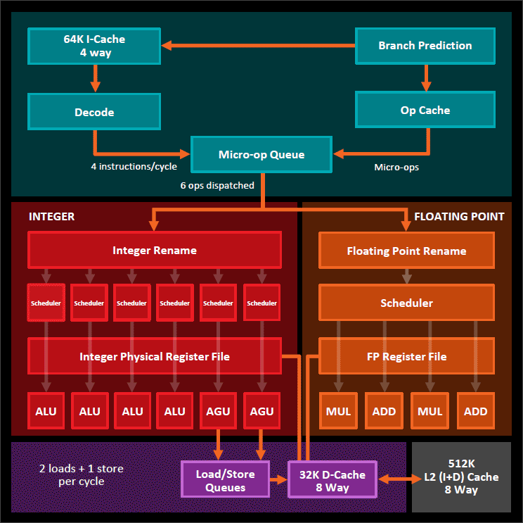
这些新的核都比推土机搭载了更多的运行资源。在整数管线上,Zen有4个算术逻辑单元(ALU)和两个地址产生单元(AGU)。浮点管线上,共享浮点单元的概念被废弃了:现在每个核都有一对独立的128位乘法叠加运算单元(FMA)。浮点单元内有分开的加法和乘法管线,用于在不进行乘法累积运算时应对更多样的混合指令。但256位AVX指令集还是得分开在两个FMA单元上执行,并动用所有的浮点单元。
这是推土机之后的巨大飞跃,从本质上讲,每个核可动用的整数和浮点运算资源都翻了个倍。然而与Broadwell和Skylake相比就不好说了。AMD的四个ALU虽然相似但不完全一样,所以有些指令必须在特定单元内处理(只有一个会算乘法,另一个会算除法),就算有其他的闲置单元也不能跨界运行。英特尔的就更加多样化,所以对于一些混合指令来说,英特尔的四个ALU实际上可能比AMD的要少。
更加复杂的是,AMD说总共六个指令可以在每周期中被发送到核的十个管线中(4个ALU,2个AGU,4个FP)。而Broadwell和Skylake都可以每周期发送八个指令。其中4个发送到AGU??Skylake有两个通用AGU和两个专用的。另外四个运算一些算数,要么整数要么浮点。
英特尔把所有功能单元分组分到四个发送端口下,编号0,1,5,6. 所有四个端口都包含一个普通的整数ALU,但端口0还含有一个AVX FMA单元、一个除法单元和一个分支单元。端口1有另一个AVX FMA单元但没有除法单元。端口5和6既没有FMA也没有除法单元。这意味着在一个周期内,处理器可以同时安排两个AVX FMA操作或是一个除法和一个AVX FMA操作,但没法同时做一个除法和两个FMA。
大体上,这说明在一个周期内,Zen可以发送四个整数运算和两个浮点运算。Skylake可以发送四个整数运算,但这需要动用所有四个端口,导致没法进行任何浮点运算。另一方面,Skylake和Broadwell都能在一个周期内同时发送四个整数运算和四个地址操作。Zen只能容纳两个地址操作。
推土机的弱点依旧如影随形
撇开区别不谈,我们就没法直接衡量这些设计的好坏。尽管如此,还是有些设计在个别方面的优势极其显著。英特尔的两种芯片都具备两个能同时启用的全256位AVX FMA单元。对于可以利用这一优势的代码来说,Skylake和Broadwell的性能都应该可以做到Zen的两倍。多年以来,AMD一直在尽力让GPU成为运行这种高强度浮点并行运算的最优选。所以某种意义上说这种差距也可以理解??但重度依赖AVX指令集的程序就会毫不犹豫地选择英特尔芯片了。
比如这在Geekbench的浮点测试SGEMM中就非常明显。这是一个矩阵乘法测试,为了最佳性能会调用AVX和FMA指令集。在单线程上,6900K管理着大约每秒900亿单精度浮点指令(90 gigaflops)。相比之下,1800X的处理速度只有53 gigaflops。虽然1800X相对更高的时钟速度有点用,但英特尔芯片在每个周期内能完成其两倍的工作量。高出来的几百兆赫不足以抵消架构区别带来的劣势。
当然,这种工作量从某种角度证明了AMD的观点:由GPU加速的相同矩阵乘法运算可以达到800以上gigaflop。如果你的计算需求包含大量的矩阵乘法,你是决不会想用慢吞吞的CPU来完成这项工作的。
AMD长期以来的难题,也是通用GPU计算的难题,就是当只有部分运算工作适合用GPU完成时该怎么办。把数据在CPU和GPU上搬来搬去会消耗额外的资源,而且这要求开发者在开发工具和编程语言间进行切换。虽然解决方法是有的,比如AMD的异构系统架构和OpenCL,但目前还没有被行业广泛采纳。
有一个Geekbench子测验从另一个角度显示了突出的优势。Geekbench有关于目前主流处理器用到的所有密码指令集的测试。在一个单线程性能测试中,锐龙碾压Broadwell-E,解码速度为4.5GB/s比2.7GB/s。锐龙有两个AES单元,都位于处理器的浮点部分。Broadwell只有一个,让AMD大大领先了。
但从单线程转到十六线程时情况就突然逆转:英特尔系统能跑到24.4GB/s而AMD只有10.2GB/s。这说明该测试在高线程数时会带宽受限,使得6900K的四存储渠道领先于1800X的双存储渠道。尽管锐龙具备更多的计算资源来进行这种运算,但当处理器干坐着等待数据传输时再多计算资源也无济于事。
至于单线程性能上,他们都输给了Kaby Lake i7-7700K。鉴于它更高的IPC和更快的时钟速度,Broadwell-E和Zen都是远远追不上的。
更高速的前端
支撑那些指令单元的是指令解码器和故障处理器。AMD在这些方面同样较推土机做出了长足的改进。就像x86处理器常做的那样,Zen先把x86指令拆解至微指令(?op)然后再安排与执行。在推土机里,重复指令(比如循环)必须被重复地读取和解码。Zen添加了一个能存储2000 ?op的微指令缓存,如此,循环中的重复指令就可以跳过解码部分。英特尔在2011年初发布的Sandy Bridge架构中首次提出了同等的数据结构。
这个架构还结合了高效的分支预测器。在处理器确切知道某个分支完成后应该执行哪个指令集之前,分支预测器会进行预先猜测。如果分支预测器预测正确,处理器的管线就可以满负荷工作;如果错误,那么就得清空管线,浪费一小部分工作量。
然而Zen的分支预测器更加机智??它大部分时候都能猜对??而且成本更低??猜错时浪费的工作量被降低了三个时钟周期。AMD现在把分支预测器称作神经网络,因为它的运作基于感知机。感知机的原理就是将一组不同权重的输入值相加,如果和大于零,感知机输出值为1,否则输出值为0.
感知机在分支预测器上起到的作用很有意思,因为它会追踪大量的输入状态然后判断某一分支是否已被占用,所以就算是长循环也很适用。推土机可能也用到了感知机,但一直到Zen的出现AMD才恍然大悟这其实是个神经网络??所以他们开始设想人工智能和施瓦辛格的愿景??让这事儿听起来无比先进。
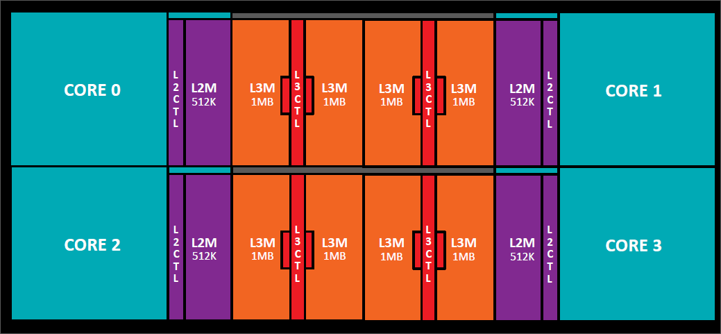
支撑这一切的是一个更大更强的缓存系统。一级缓存是回写式缓存(而不是推土机的透写式),所以速度更快,存储的传输负载更小。一级和二级缓存都可以带来两倍于推土机的带宽,而三级缓存可以带来五倍,但也更加复杂。CCX内的每个核都有2MB的三级缓存 ,所以每CCX共有8MB,整个处理器共16MB。缓存是共享的,但读取速度不尽相同。离缓存最近的核自然读取速度最快,另外三个会稍慢一些。
AMD把CCX之间互相沟通用到的技术叫做Infinity Fabric。AMD对此做出的描述不甚清晰,但基本原理就是它是CCX之间一个原本可用在CCX内的高速缓存一致性的接口和总线??电源管理微控制器、安全微控制器、扩展插口标准控制器和存储控制器都与它相接。它甚至可以被用在母板插口之间。
至少在多插口的情况中,AMD把Infinity Fabric称为“改良版的相关性超传输(Coherent HyperTransport),”但有时候AMD又说这不是基于超传输。
比上面这些都更加重要的是,Zen支持同时多线程(SMT)。几乎核内所有资源都可被“竞争性共享”,也就是说在没有第二个线程的时候,第一个线程通常可以占用全部的运行资源。指令发送遵循循环制,所有周期轮流在轮流的线程上运行。
SMT带来的收益因情况而异。Cinebench显示启用SMT带来了良好的提升,跑分高出40%多。然而这大大取决于工作量,多线程Geekbench启用SMT后只提高了不到10%。虽然一般来说SMT是绝对赢家??拉高了多线程程序的速度又不损失单线程的性能??但我们也注意到,游戏杀手47(Hitman)因为启用SMT流失了10%的帧速率。
除了运行资源分配大不相同外,总体规律就是Zen上运行的所有工作都还是要比基于单个周期的英特尔设计慢一些。(我们估计落后于Broadwell 5%,落后于Skylake 15%。)但Zen的更高时钟速度加上可靠的同时多线程设计意味着它可以比肩Broadwell-E。比如在Cinebench R15中,1800X和6900X在单线程测试中持平,在多线程测试中比英特尔芯片高出6%。在单线程Geekbench 4中,AMD处理器依然与英特尔持平,虽然多线程上落后英特尔20%。这是在不同测试中由不同混合指令集和不同带宽依赖度带来的反馈。
据此,AMD达成了它的IPC指标,水平与英特尔耗时两年半的芯片设计已经相当靠近。多亏了时钟速度与核数,这意味着Zen在各种不同运行量量级上都能够与英特尔势均力敌。
高效的引擎
相比于挖掘机,Zen的能耗也有大幅降低。
如果说把IPC拉高了52%已经非常惊艳的话,那么降低能耗这方面更是有过之而无不及:在多线程Cinebench上,AMD声称效能功耗比提高了269%。同功耗下,Zen的跑分是挖掘机的3.7倍。
能源效率的提高来自于很多方面。一项重大的突破出自AMD自己之手:效能功耗比自切换到GlobalFoundries的14纳米鳍式场效应晶体管工艺(FinFET)后上升了70%(就算GlobalFoundries跟不上的话,AMD也已经证实了三星14纳米工艺的可用性);甚至面向移动端的挖掘机处理器目前也是基于古董级的28纳米工艺。此外其他方面的提高要归功于AMD的工程师。
129%的提高来自更优的新架构设计。不仅运行速度更快,而且更加节能。微指令缓存不仅减轻了读取和解码指令的压力,而且降低了能耗。从微指令缓存直接读取比从一级指令缓存读取再运行解码器所消耗的资源要少得多。类似地,改良版的分支预测器意味着处理器在预测错误后在错误分支上浪费的时间更少,浪费的能源也就更少。
整数核还带有提高性能与效率的特性。最常见的x86指令就是移动指令,把数据从存储器搬到寄存器上,从这个寄存器搬到那个寄存器上,从寄存器搬到存储器上。那些寄存器之间的数据移动已经被整数核取消了,取而代之的是寄存器重命名,这个技巧曾被首次用在推土机上。
x86还包括操纵堆栈的指令;这些指令会一边从存储器读写数据一边在特定寄存器上加减数据(堆栈指针)。推土机采用了一些堆栈的特殊处理,用以降低堆栈相关指令之间的依赖度(从而扩大并行运算的规模),而Zen配有一个更加复杂的堆栈引擎,它可以取消某些堆栈操作指令。这同时改良了性能(同样是通过更大的并行运算规模)且降低了能耗。
核心设计的大大优化也为降低能耗做出了贡献。集成电路由多种不同的标准单元构成,比如NAND和NOT逻辑门,触发器,甚至是更复杂的元素,比如半加器和全加器。这其中的每个组成部分(叫做标准单元)都可以接受多种不同的设计,从而在性能、尺寸和耗能上权衡利弊。
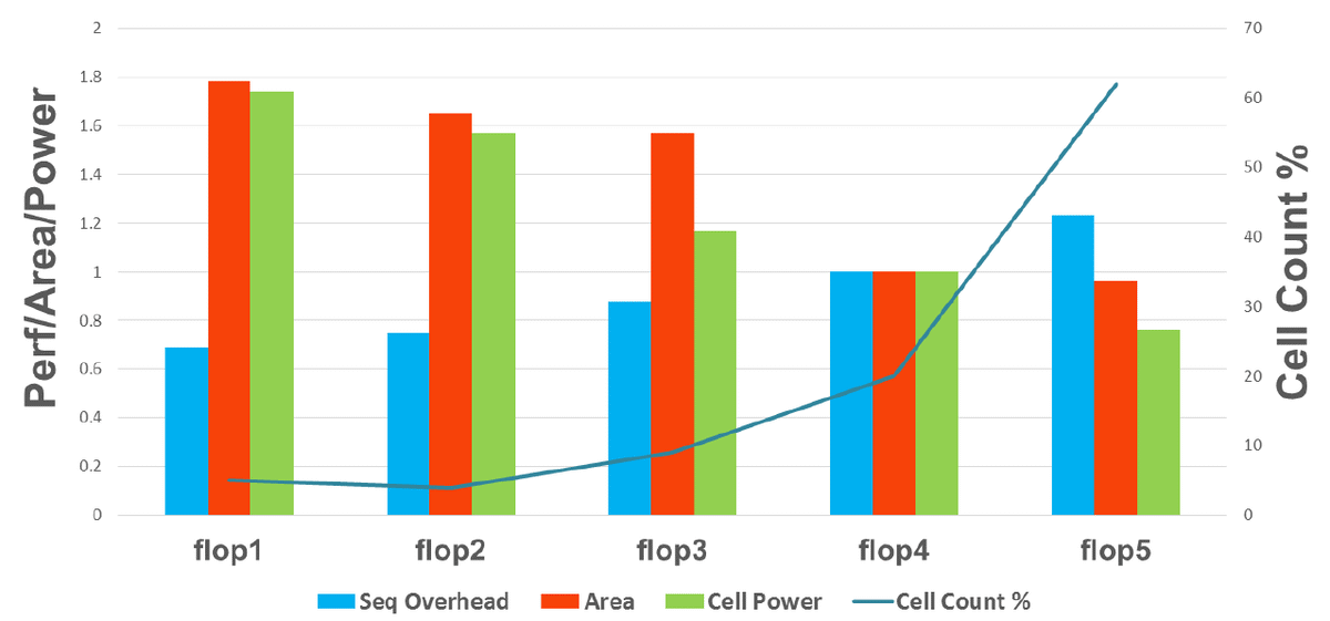
大多数的Zen所用的都是图中右边所示的速度慢但更高效的触发器
AMD建立了一个很大的标准单元库,不同的标准单元特性各异。比如他们有五种不同的触发器设计。最快的速度是最慢的两倍,但最快的版本的资源占用率要高出80%,耗能也是后者的两倍。凭借这么大一个库,优化后的Zen在必要之处装配了较快较大较高性能的部件,在可妥协之处用上了稍小稍慢但更高效的部件。在Zen的架构中,只有不到10%的触发器用了高性能设计,而60%的时候都在用效率更高的那种。
最终的成果就是在关键路径部分的性能和其他部分的效率之间达到了完美的平衡。
电源管理
Zen的电源管理方式很复杂也很强大。像现今其他的处理器一样,它采用了大量门控时钟,会把芯片上没有用到的部分暂时关闭。但在这之上,它还有一个集成电源管理控制器,用于监测每个核的电压并根据温度和负载进行调整。AMD把这个系统叫做SenseMI(MI为机器智能machine intelligence)。
就像英特尔在Skylake上的手法一样,Zen把电源管理任务从软件和操作系统上剥离,将其融合到硅芯片中。操作系统对处理器电源管理事件做出反应需要几十或几百微秒;而芯片上的硬件只需要几微秒。这能够形成对电压和时钟速度更紧密的控制。又跟Skylake类似的是,操作系统负责设置芯片的粗粒度功率??它可以压低几百甚至几千兆赫??但满负荷运转时(电源状态P0),控制权又会交回到处理器手上。
每个CCX上布满了各种传感器:20个热敏二极管,48个电源监控器,9个电压下降检测器,还有1300多个关键路径监控器。这些传感器都与Infinity Fabric控制面板相连,向电源管理单元传输数据,每秒汇报读数1000次,精度分别达到1mA, 1mV, 1mW, 1°C。
另一方面,这个系统使得Zen只需要能维持正常运作的最小值电压。每个核都配有自己的调压器,所以它们都会保持在时钟速度达标时的最低电压。不是所有核都生来平等,有些天生就比别人跑得快。那些速度快的核就会被分配到较少的功率,留出能量净空给其他速度慢的核提速。以相同速度运行时,速度快的核能够比速度慢的核功耗低5%。
我们可以拿这种单核调整技术与AMD之前的自适应电压与频率调节(AVFS)作比较,后者整个芯片上的电压都是统一设置的。在以前,电压必须高到足以支持所有的核。类似地,英特尔的核都共享同一个电源层并在同一电压下工作。因核而异的电压调节会更节能。
Zen的稳压用的是基于芯片的低压差线性稳压器(LDO)。英特尔的Haswell和Broadwell用的也是基于芯片的稳压器,但那是更复杂而低效的一种(全集成式电压调节模块,FIVR)。理论上来说,英特尔的系统比AMD可以应对更广的核电压范围,但在实际操作中,AMD说这种功能其实用处不大。所有的核都差不多在同一电压下工作,所以LDO是更好的选择。Skylake应该会放弃FIVR,把稳压器移回母板;这使他们没法打造那种AMD吹捧的Zen的高速微调:比如要是电压跌至过低,Zen就会放慢该核的时钟速度直到它恢复为止。
伴随25MHz增量,Zen时钟速度可以在其标准时钟和提升的最大值之间平滑变化
将电压拼命压低到维持预设频率的最小电压值的另一对应版本是,推高频率直至刚好达到预设功耗。压低功耗的控制系统也可以同样被用来推高每个核的时钟速度,从而最大化利用处理器的功率开支。这种涡轮增压(英特尔的睿频)也并不是什么新鲜玩意了,但AMD系统的精细频率提速(Precision Boost)倒是有些令人眼前一亮的特点。首先这种提速是细粒度的,能够精确控制时钟速度到每25MHz的频率。
其次,如果传感器发现还有富余的能量净空,时钟速度就可以被推到标准提速极限以上,AMD把这叫做自动超频技术(Extended Frequency Range,XFR)。如果散热片和冷却器远超最小规格使得芯片工作得很悠闲,XFR就会继续上推时钟速度,1800X和1700X的增加上限是100兆赫,1700的上限是50兆赫,基本上算是“免费”加了一个小小的超频。
另外70%的性能功耗比的提升便是来源于这些在供能分布、时间和电压上的完善和优化。
然而到了“真的”超频的时候,R7处理器就好坏参半了。一方面,这些处理器都解锁了cpu倍频,至少在与合适的芯片集搭配使用时是这样,那么你就可以用它做任何尝试。AMD估计只要抬高到1.45V,大多数1800X用全八核都能够跑到4.2GHz。但是AMD也说了1.45V可能会缩短芯片寿命。
启用超频模式也会损失一些节能特性。比方说,你不可能在能量限制下让XFR额外提速200MHz,你也不能让一个1800X以3.8GHz的基础速度运行外加一个4.2GHz的睿频提速(两者同时提升200兆赫)。一旦超频被启用,处理器就只能以固定速度运行了(电源状态P0情况下)。
这和英特尔不一样,睿频加速技术可以让你具体设置1、2、3或4核提速,Kaby Lake甚至能让你在AVX密集的工作中用个小体量的加速器。这在超频模式下运作得十分简洁干脆,像正常运行下的Zen一样巧妙。
无芯片集的芯片集平台
锐龙R7绝不仅仅是个处理器,它是基于芯片的系统。但它到底有没有被这么用就取决于它匹配了哪种母板和芯片集。
处理器本身有20个PCIe 3.0通道,4个第一代USB 3.1(5GB/s)控制器,外加4个PCIe和输入输出的混合通道;这些可以被分到单个x4 NVMe设备中,或分开到2个SATA 外加一个x2 NVMe中,或是2个SATA外加x2 PCIe。此外还有2个DDR4存储渠道。
在这20个PCIe 3.0通道中,四个一般用于与芯片集沟通。AMD有三个常用芯片集;高端的X370, 中端的B350,以及低端的A320. 它们都带有第二代USB 3.1(10Gb/s)控制器(X370和B350含两个,A320含一个),一些额外的SATA控制器(X370含4个,B350含2个,A320含2个),2个SATA Express端口(也可以被用作4个SATA 3.0端口),以及一些PCIe 2.0通道(三个版本分别含8个,6个,4个)。X370和B350都可启用超频,X370还允许处理器上剩余的16个PCIe 3.0通道分成两组8通道用于双GPU支持。
但对于小型系统而言,额外的输入输出通道和加大版的芯片集并不符合需求。于是就有了另外两种芯片集,X300和A/B300,它们作为芯片集的意义大大下降:唯一的输入输出功能是处理器本身自带的,没有第二代USB 3.1,没有SATA Express,没加任何PCIe 2.0通道。这种芯片集只提供了为数不多的几个功能,主要是围绕安全和可信任平台模块(Trusted Platform Module)的配置。正因如此它们长得非常迷你,AMD说它们能被安装在指甲那么大的芯片上。
由于这些芯片集只能做这么点事情,它们不需要处理器上的四个PCIe通道,而是配有专供的SPI链接。这意味着处理器上的20个PCIe通道都可用,连X300也可以做到超频和双GPU支持。
撇开芯片集不管,AMD打算在2020年前始终采用同一个插口Socket 1331和同一个平台AM4,除非有什么新科技的诞生(比如PCIe 4.0或DDR5)迫使它更换组件接脚分布。锐龙AM4母板能够适配现在的AM4 APU,也能适配今年即将面世的Raven Ridge 基于Zen处理器的APU。这就是为什么就算是现在的锐龙处理器没法用,几乎所有Zen母板还是搭载了集成显示输出。
AMD的赌注开始回本
很显然Zen架构比推土机不知道高到哪里去了。推土机和AMD现有的产品根本没法比,而且它早已被一骑绝尘的英特尔甩出十万八千里。但Zen不一样。AMD的新架构不仅在性能上可以媲美英特尔的Broadwell,而且十分高效。
但到底要不要买Zen是个复杂的问题,这个复杂跟推土机为什么会那么弱的很多原因是一样的。对于多线程密集的工作,Zen比Broadwell的性价比高很多,且性能不相上下。有时候Broadwell-E会更快一点而有时候Zen会更快一点,但在那些尤其依赖AVX或存储带宽的工作上,Zen具有压倒性优势。这使得AMD 499美元的芯片成为英特尔 1049美元的芯片的完美替代品。
我猜开发者会非常渴望能尽快用上Zen。软件编译(尤其是C++的程序)很容易多线程化,而且几乎无一例外地依靠CPU,所以核数和线程数的翻倍造就了巨大的性能优势。AMD用同一套逻辑去吸引的另外一群受众是做电视游戏视频流的人:多核的芯片才有能力一边玩游戏一边进行高质量的视频压缩,而这正是英特尔四核芯片的弱点。
但在其他工作中,英特尔更优的单线程性能更被看重。包括Grand Theft Auto V, Battlefield 4, 以及 Ashes of the Singularity在内的游戏中,Kaby Lake i7-7700K能领先于1800X,就算它只有后者一半的核数和线程数。
就跟当初卖推土机的时候一样,AMD希望开发者们打造的软件能在多核芯片上扩展升级,多给Zen机会去表现出它优于英特尔的长处。但Steam Hardware问卷调查清楚地说明了为什么至少在短期内开发者还不会这么做,毕竟双核和四核处理器占据了绝大多数游戏系统。
但很大一个区别在于,Zen就算不在最佳状态下依旧表现优异。i7-7700K能在个别工作中带来稍高的帧率和稍强的性能,但推土机对于单线程任务来说简直就太尴尬了,可Zen还是做得挺好??好到你也许会愿意牺牲一部分程序的最顶级效果来换取其他程序中的巨大性能提升。
AMD已经很久很久没这么风光了。多年以来认准英特尔的PC发烧友们从不用纠结该买谁家的处理器,但AMD终于带来了绝对值得一看的产品。也许它还不是所有人理想中的芯片,但至少这次,它终于能为一部分人理想中的芯片了。
以下是原文:
Before the company’s new Zen offerings, it’s fair to say that AMD’s last attempt at building a performance desktop processor was not tremendously successful.
The Bulldozer core released in 2011 had a design that can, at best, be described as idiosyncratic. AMD made three bets with Bulldozer: that general purpose workloads would become increasingly multithreaded, that floating point intensive workloads would become increasingly GPU-driven, and that it would be able to aggressively scale clock speeds.
Accordingly, AMD created processors with oodles of simultaneous threads, relatively long pipelines, relatively narrow pipelines, and relatively few floating point resources. The idea was that clock speed and the GPU would make up for the narrowness and lack of floating point capability. AMD hoped all those threads would be working hard.
Each Bulldozer module could run two threads simultaneously, with two independent integer pipelines and one shared floating point pipeline within a module. Desktop processors shipped with two, three, or four modules for four, six, or eight threads in total. Compared to Bulldozer’s predecessor, the K10, each integer pipeline was narrow: two arithmetic logic units (ALUs) and two address generating units (AGUs), instead of three of each in K10. So, too, was the floating point pipeline, with two 128-bit fused multiply-add (FMA) units that could be paired together to perform a single 256-bit AVX FMA instruction. AMD designed the processor with a base clock speed goal of 4.4GHz.
Bulldozer? Bullshit, more like
None of AMD’s gambles paid off. The high-end desktop parts, with their four modules and eight threads, had an abundance of integer threads. But most consumer workloads still can’t be distributed evenly across eight threads. Single-threaded performance continues to matter a great deal. On the other hand, the sharing of the floating point units means that applications stuffed with floating point arithmetic have too few resources to work with. While GPU-based computing is important in certain workloads?such as scientific supercomputing?mainstream applications still require the CPU for floating point number crunching. Bulldozer leaves them short.
Even these issues might have been tolerable if the clock speed goals had been reached. A processor can get away with low instructions per cycle (IPC) if it runs at a high enough clock speed, but AMD came nowhere close to its 4.4GHz base goal. The top-end, four-module part had a base frequency of 3.6GHz. It could boost up to 4.2GHz under reduced workloads. This is a long way short of the design goal.
As a result, the first Bulldozer processors were in many workloads slower, yet more expensive, than their K10 predecessors. They were wholly uncompetitive with contemporaneous Intel parts.
AMD did iterate the design. The top-end second generation Bulldozer, named Piledriver, boosted the base clock up to 4.7GHz and up to 5.0GHz boosted. Combined with some internal improvements, this made it about 40 percent faster than the top Bulldozer. This came at a power cost, however: to hit those clock speeds, the processor drew 220W, compared to 125W for the Bulldozer.
The third-generation Steamroller made improvements to IPC and gained about nine percent over Piledriver. Fourth-generation Excavator added as much as 15-percent IPC over Steamroller. However, neither Steamroller nor Excavator were used in high-end desktop processors. The performance desktop space was ceded entirely to Intel.
AMD did use Steamroller and Excavator in some of its APUs?”Accelerated Processing Units,” which is to say, CPUs with integrated GPUs. But even in this space, the Bulldozer family has proved limiting. Mobile-oriented APUs in the 10-25W space only have one Excavator module (two threads). Their performance is substantially lower than that of Intel’s chips in the same power envelope, and Intel manages to squeeze four threads (albeit only on two cores) onto its low-power processors.
And to reach the ultra-low-power 3-7W space, AMD offers nothing at all with a Bulldozer-family core. The company has had chips operating in very low-power envelopes, but these have all used derivatives of the Bobcat core. This is a completely different processor design, developed for mobile and low-power operation. Bobcat derivatives are also used in the PlayStation 4, PlayStation 4 Pro, Xbox One, and Xbox One S.
By comparison, Intel’s designs run the gamut (albeit with staggered release schedules); its Broadwell design ranges from two-core, four-thread mobile parts with a power draw of as little as 3.5W, up to 22-core, 44-thread server chips drawing 145W (or higher clocked 12-core, 24-thread parts drawing 160W).
Time for something new
By 2013, AMD had realized that Bulldozer was never going to be the processor that the company wanted it to be. A new architecture was necessary. AMD had a few particular goals for this: the new architecture had to be a viable challenger in the high-end desktop market, and it had to offer at least 40 percent better IPC than Excavator.
Like Intel before it, AMD wanted its new design to span the full range from fanless mobile through server and high-end desktop. So this improved IPC needs to be wedded to improved power efficiency. But AMD isn’t giving up on the Bulldozer ideas completely: the company still believes that high numbers of multiple simultaneous threads are the future, and some of the design decisions suggest that AMD still sees GPUs as being central to serious floating point number crunching.
Four years in the making, the Zen core is the result of this new approach. And where Bulldozer failed to meet its objectives, AMD says that it has soundly beaten its 40-percent IPC improvement goal. In the single-threaded Cinebench R15 benchmark at a constant 3.4GHz, Zen achieves a score 58-percent higher than Excavator and 76-percent better than Piledriver. The typical IPC improvement, when compared to Excavator, is around 52 percent. It does this at significantly lower power draw, too: in multithreaded Cinebench R15, the performance per watt is more than double what it was for Piledriver.
Compared to the Bulldozer family, Zen is so much better across the board that it makes for an interesting?if uneven?competitor to what Intel is offering. Years have passed since AMD could even hope to be considered a performance rival to its much larger competitor, but with Zen, AMD finally has an architecture that can compete.
What makes it tick
The basic building block of Zen is the Core Complex (CCX): a unit containing four cores, capable of running eight simultaneous threads. True to AMD’s belief in high core and thread counts for desktop processors, the first Ryzen 7 series processors include two CCXes, for a total of eight cores and 16 threads. Three versions are launching: the 1800X, a 3.6-4.0GHz part at $499/?490, the 1700X, 3.4-3.8GHz at $399/?390, and the $329/?320 1700 at 3.0-3.7GHz.
In the second quarter, these will be joined by Ryzen 5. The R5 1600X will be a six-core, 12-thread chip running at 3.6-4.0GHz (two CCXes, with one core from each disabled), and the 1500X will be a four-core, eight-thread chip at 3.5-3.7GHz (just a single CCX).
Zen scales up, too. At some point this year, AMD will launch server processors, codenamed “Naples,” containing eight CCXes for a total of 32 cores and 64 threads.
This design decision already sets AMD apart from Intel. Intel’s processor range is strangely bifurcated. The company’s latest core is Kaby Lake, but Kaby Lake is only available in two- and four-core versions, some with simultaneous multithreading (SMT), others without. To go beyond four cores, you have to switch to a previous-generation architecture: Broadwell.
Broadwell, a 14nm shrink of the previous Haswell architecture, was first introduced in September 2014. Currently, every processor that’s “bigger” than a four-core, eight-thread mainstream desktop or mobile part is built using the Broadwell core. This includes not just the enthusiast-oriented Broadwell-E parts that offer six, eight, or 10 cores and 12, 16, or 20 threads. It also includes Broadwell-EP server parts, right up to the Xeon E7-8894V4 that was launched just two weeks ago. This is an 8-socket-capable 24-core, 48-thread chip that won’t give you much change from $9,000.
These first Ryzen processors straddle that discontinuity in the Intel line-up. The R7 1700 is going more or less head to head with the Kaby Lake i7-7700K. The latter uses Intel’s refined 14nm process and newest architecture with the best single-threaded performance, running at 4.2-4.5GHz. But the 1800 and 1800X are competing against Broadwell designs, the six-core, 12-thread 3.6-3.8 GHz i7-6850K ($620/?580 or so) and eight-core, 16-thread 3.2-3.7 GHz i7-6900K ($1,049/?1,000 or so), respectively. In upping the core count, Intel’s forcing you to sacrifice its latest core and most power efficient process and to switch to older, less frequently updated chipsets to boot (the current X99 dates back to late 2014).
Bigger, beefier cores
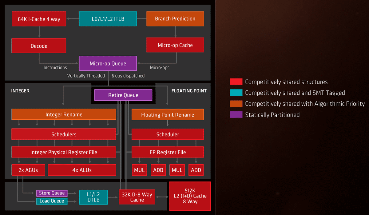
Zen core block diagram.
Each of those new cores is equipped with many more execution resources than Bulldozer. On the integer side, Zen has four ALUs and two AGUs. On the floating point side, the shared floating point unit concept has been scrapped: each core now has a pair of 128-bit FMA units of its own. The floating point units are organized as separate add and multiply pipes to handle a more diverse instruction mix when not performing multiply-accumulate operations. But 256-bit AVX instructions have to be split up across the two FMA units and tie up all the floating point units.
This is a big step up from Bulldozer, essentially doubling the integer and floating point resources available to each core. Compared to Broadwell and Skylake, however, things are murkier. AMD’s four ALUs are similar to each other though not identical; some instructions have to be processed on a particular unit (only one has a full multiplier, only one has a divider), and they can’t be run on other units even if they’re available. Intel’s are a bit more diverse, so for some instruction mixes, Intel’s four ALUs may possibly be lesser than AMD’s.
Complicating this further, AMD says that six instructions total can be dispatched per cycle across the 10 pipelines (four ALU, two AGU, four FP) in the core. Broadwell and Skylake can both issue eight instructions per cycle. Four of those go to AGUs?Skylake has two general-purpose AGUs and two more specialized ones. The other four perform arithmetic of some kind, either integer or floating point.
Intel groups its functional units behind four dispatch ports, numbered 0, 1, 5, and 6. All four ports include a regular integer ALU, but port 0 also has an AVX FMA unit, a divider, and a branch unit. Port 1 has a second AVX FMA unit but no divider. Ports 5 and 6 have neither an FMA nor a divider. This means that in one cycle, the processor can schedule two AVX FMA operations or one divide and one AVX FMA. But the processor can’t do a divide and two FMAs.
In principle, this means that in one cycle, Zen could dispatch four integer operations and two floating point operations. Skylake could dispatch four integer operations, but this would tie up all four ports, leaving it unable to also dispatch any floating point operations. On the other hand, Skylake and Broadwell could both dispatch four integer operations and four address operations in a single cycle. Zen would only manage two address operations.
Bulldozer’s foibles aren’t quite a thing of the past
Isolating these differences to measure the impact of the designs is nigh impossible. Nonetheless, there are a few areas where the advantage of one design or the other is clear. Intel’s chips both have two full 256-bit AVX FMA units that can be used simultaneously. For code that can take advantage of this, Skylake and Broadwell’s performance should easily double Zen’s. For many years, AMD has been pushing the GPU as the best place to perform this kind of floating point-intensive parallel workload. So on some level this discrepancy makes sense?but programs that depend heavily on AVX instructions are likely to strongly favor the Intel chips.
This becomes visible in, for example, one of Geekbench’s floating point tests, SGEMM. This is a matrix multiplication test that uses, when available, AVX and FMA instructions for best performance. On a single thread, the 6900K manages about 90 billion single precision floating point instructions per second (gigaflops). The 1800X, by contrast, only offers 53 gigaflops. Although the 1800X’s higher clock speed helps a little, the Intel chip is doing twice as much work with each cycle. A few hundred megahertz isn’t enough to offset this architectural difference.
Of course, this is the kind of workload that in some ways proves AMD’s point: GPU-accelerated versions of the same matrix multiply operation can hit 800 or more gigaflops. If your computational requirements include a substantial number of matrix multiplications, you’re not going to want to do that work on your CPU.
The long-standing difficulty for AMD, and for general purpose GPU computation in general, is how to cope when only some of your workload is a good match for the GPU. Moving data back and forth between CPU and GPU imposes overheads and often requires developers to switch between development tools and programming languages. There are solutions to this, such as AMD’s heterogeneous systems architecture and OpenCL, but they’re still awaiting widespread industry adoption.
One particular Geekbench subtest showed a strong advantage in the other direction. Geekbench includes tests of the cryptographic instructions found in all mainstream processors these days. In a test of single-threaded performance, the Ryzen trounces the Broadwell-E, encrypting at 4.5GB/s compared to 2.7GB/s. Ryzen has two AES units that both reside within the floating point portion of the processor. Broadwell only has one, giving the AMD chip a big lead.
This situation is reversed when moving from one thread to 16: the Intel system can do 24.4GB/s while the AMD only does 10.2GB/s. This suggests that the test becomes bandwidth-limited with high thread counts, allowing the 6900K’s quad-memory channels to give it a lead over the 1800X’s dual channels. Even though the Ryzen has more computational resources to throw at this particular problem, that doesn’t help when the processor sits twiddling its thumbs waiting for data.
And when it comes to single-threaded performance, the Kaby Lake i7-7700K pulls well ahead of both platforms. With its combination of superior IPC and faster clockspeeds, neither Broadwell-E nor Zen can keep up.
Faster front-end
Feeding those instruction units are the instruction decoder and out-of-order machinery. Again, AMD has made substantial improvements relative to Bulldozer. As is now the norm among x86 processors, Zen decodes x86 instructions into micro-ops (?op) that are then scheduled and executed within the processor. In Bulldozer, repeated instructions (such as those in a loop) would have to be repeatedly fetched and decoded. Zen adds a ?op cache storing 2,000 ?ops so that loops can bypass the decoding. Intel first introduced an equivalent data structure in its Sandy Bridge architecture released at the start of 2011.
This is combined with a much smarter branch predictor. Branch predictors try to guess which instructions will be executed after a branch before the processor actually knows for sure. If the branch predictor guesses correctly, the processor’s pipelines can be kept full. If not, it will have to flush its pipelines and waste some amount of work.
The Zen branch predictor is smarter?it guesses correctly more of the time?and cheaper?the penalty of an incorrect guess has been reduced by three cycles. AMD now describes the branch predictor as being a neural network because it’s based on perceptrons. A perceptron takes a number of weighted inputs and adds them together. If their sum is greater than zero then the perceptron’s value is 1. Otherwise, that value is 0.
Perceptrons are interesting for branch predictors because they can track lots of input states to provide their decision on whether a branch is taken or not taken. This makes them a good match even for long loops. Bulldozer is suspected to use perceptrons, too. But it’s only with Zen that AMD seems to have cottoned on to the fact that you can call this a neural net?and hence bring to mind visions of artificial intelligence and Arnold Schwarzenegger?making the thing sound incredibly advanced.
Feeding all this is a bigger, better cache system. The level 1 cache is now a write-back cache (instead of Bulldozer’s write-through), which makes it faster and reduces memory traffic. The level 1 and 2 cache both offer about twice the bandwidth than in Bulldozer. The level 3 cache offers five times the bandwidth, and it’s also more complex. Each core within a CCX has 2MB of L3 cache, for 8MB across the CCX and 16MB across the entire processor. This cache is shared, but the speed at which it can be accessed will vary. The cache slice closest to a core is, naturally, the fastest. The other three are a little slower.
A big chunk of each CCX is cache.
Communication between the CCXes uses what AMD calls the Infinity Fabric. AMD is a little opaque when describing this. The basic principle is that this is a high-speed, cache-coherent interface and bus which can be used within a CCX?the power management and security microcontrollers both connect to it, as do PCIe and memory controllers?between CCXes. It can even be used between sockets on a motherboard.
At least for multisocket situations, AMD describes Infinity Fabric as “Coherent HyperTransport plus enhancements,” but on other occasions the company has said it isn’t based on HyperTransport.
To top it all off, Zen supports simultaneous multithreading. Almost all the resources in the core are “competitively shared,” which means that in the absence of a second thread, the first thread should generally be able to use all the available execution resources. Instructions are dispatched on a round robin basis, with alternate cycles executing from alternate threads.
Gains from SMT varied. Cinebench showed healthy improvement, scoring some 40 percent higher just from having SMT enabled. This is highly workload dependent, however; multithreaded Geekbench saw a boost of just under 10 percent from enabling SMT. While SMT is normally a big win?a free boost to multithreaded programs at no real detriment to single-threaded ones?we did notice that Hitman (2016) shed around 10 percent of its framerate from having SMT enabled.
Apart from situations in which the difference in execution resources is significant, the general pattern is that all of this work on Zen leaves it a little slower than Intel’s designs on a per-cycle basis. (Let’s estimate five percent behind Broadwell and 15 percent behind Skylake.) But a combination of higher clock speeds and a solid simultaneous multithreading implementation means that it can keep up with the Broadwell-E. In Cinebench R15, for example, the 1800X ties with the 6900X in single-threaded tests, and it’s about six percent better than the Intel chip in multithreaded. In single-threaded Geekbench 4, the AMD processor again ties the Intel one, though its multithreaded performance trails Intel by about 20 percent. This is a reflection of the different instruction mix and bandwidth dependence of the different tests.
Accordingly, AMD has beaten its IPC goal relative to Bulldozer and is within spitting distance of Intel’s two-and-a-half-year-old design. Thanks to the clock speed and core count, this means Zen is competitive with Intel across a wide range of workloads.
Efficient engine
Relative to Excavator, Zen does this at a significant reduction in power usage, too.
If boosting IPC by 52 percent was impressive, the power reduction is even more so: in multithreaded Cinebench, AMD claims that performance per watt has increased by 269 percent. For the same power draw, Zen scores 3.7 times what Excavator achieved.
That efficiency improvement comes from a range of sources. One big improvement is out of AMD’s hands: performance per watt is improved by 70 percent from the switch to GlobalFoundries’ 14nm FinFET manufacturing process (and should GlobalFoundries falter, AMD has validated the design on Samsung’s 14nm process too); even mobile-oriented Excavator parts are currently built on a now-ancient 28nm process. But the rest of the improvement is down to AMD’s engineers.
Some 129 percent of the improvement is attributed to the new, better architecture. As well as being a lot faster, it’s also more efficient. That ?op cache doesn’t just relieve the burden on instruction fetching and decoding; it also saves power. It’s cheaper to read from the ?op cache than to read from the level 1 instruction cache and then run through the decoder. Similarly, the improved branch predictor means that the processor spends less time speculatively executing the wrong branch, a task that represents wasted energy.
The integer cores also include features that help performance and boost efficiency. Some of the most common x86 instructions are move instructions that copy data from memory to register, register to register, or register to memory. These register to register moves are eliminated by the core, replaced instead by register renaming, a trick first used in Bulldozer.
x86 also includes instructions that are dedicated to manipulating the stack; these instructions will simultaneously read or write a value from memory and add or subtract from a dedicated register (the stack pointer). While Bulldozer includes some special handling of the stack to reduce the dependencies between instructions using the stack (thereby improving the scope for parallel execution), Zen includes a more complex stack engine that can eliminate certain stack manipulation instructions. This both improves performance (again, by allowing more parallel execution) and reduces power usage.
The design of the core was also extensively optimized to use less power. Integrated circuits are built of a variety of standard units such as NAND and NOT logic gates, flipflops, and even more complex elements such as half and full adders. For each of these components (called standard cells), a range of designs is possible with different trade-offs between performance, size, and power consumption.
Fast flipflops, on the left, are large and power-hungry. Most of Zen uses slower, more efficient ones, on the right.
AMD built a large library of standard cells with different characteristics. For example, it has five different flipflop designs. The fastest is twice as fast as the slowest, but it takes about 80 percent more space and uses more than twice as much power. Armed with this library, Zen was optimized to use the smaller, slower, more efficient parts where it can and the faster, larger, high-performance parts when it must. In Zen, the high-performance design is used for fewer than 10 percent of the flipflops, with the efficient one used about 60 percent of the time.
The result is a careful balance of performance in the critical paths where it matters and efficiency where less performance is needed.
Power management
Zen’s power management is complex and capable. Like any other modern processor, it’s aggressively clock gated, enabling unused areas of the chip to be temporarily turned off. But more than that, it has an integrated power management controller that monitors and adjusts the voltage used by each core according to temperature and loading. It’s a system that AMD is calling SenseMI (where “MI” stands for “machine intelligence”).
Just as Intel did with Skylake, this takes most power management roles out of the hands of software and the operating system, and it bakes them into silicon. Operating systems can respond to processor power management events in tens or hundreds of milliseconds; hardware on the chip can respond in just a handful of milliseconds. This allows much tighter control over voltages and clock speeds. And again, like Skylake, the operating system is responsible for setting the coarse-grained power of the chip?it can throttle the whole thing back by many hundreds or even thousands of megahertz?but when operating at maximum performance (the “P0” power state), control is turned over to the processor itself.
Scattered across each CCX are a whole bunch of sensors; 20 thermal diodes, 48 power supply monitors, nine voltage droop detectors, and more than 1,300 critical path monitors. These sensors are all connected to an Infinity Fabric control plane, feeding their data into a power management unit.They report their readings 1,000 times a second, and are accurate to 1mA, 1mV, 1mW, and 1°C.
On the one hand, this system allows Zen to cut back its voltages to the bare minimum needed to operate correctly. Each core has its own voltage regulator, and they’ll be set as low as possible to maintain clock speeds. Not all cores are created equal; some are naturally faster than others. Those faster cores are given slightly less power, creating the thermal headroom to boost the power given to other, weaker cores. A fast core can use as much as five percent less power than a slow one at the same speed.
This per-core adjustment is in contrast to AMD’s previous Adaptive Voltage and Frequency Scaling (AVFS) implementations, where the voltage was set chip-wide. In the past, the voltage had to be high enough to support all the cores. Likewise, Intel’s cores all share a power plane and operate at the same voltage. Setting it on a core-by-core basis saves power.
The voltage regulation uses on-chip low drop-out (LDO) linear regulators. Intel’s Haswell and Broadwell also used on-chip regulators of a more complex, less efficient type (FIVRs, fully integrated voltage regulators). In principle, Intel’s system can handle a wider range of core voltages compared to AMD, but in practice, AMD said that this capability wasn’t particularly useful. All the cores operate at about the same voltage, so the LDO was a better approach. Skylake is believed to drop the FIVRs, moving voltage regulation back onto the motherboard; this precludes making the kind of high-speed fine adjustment that AMD claims for Zen. If the voltage droops too low, Zen will slow a core’s clock speed while it recovers.
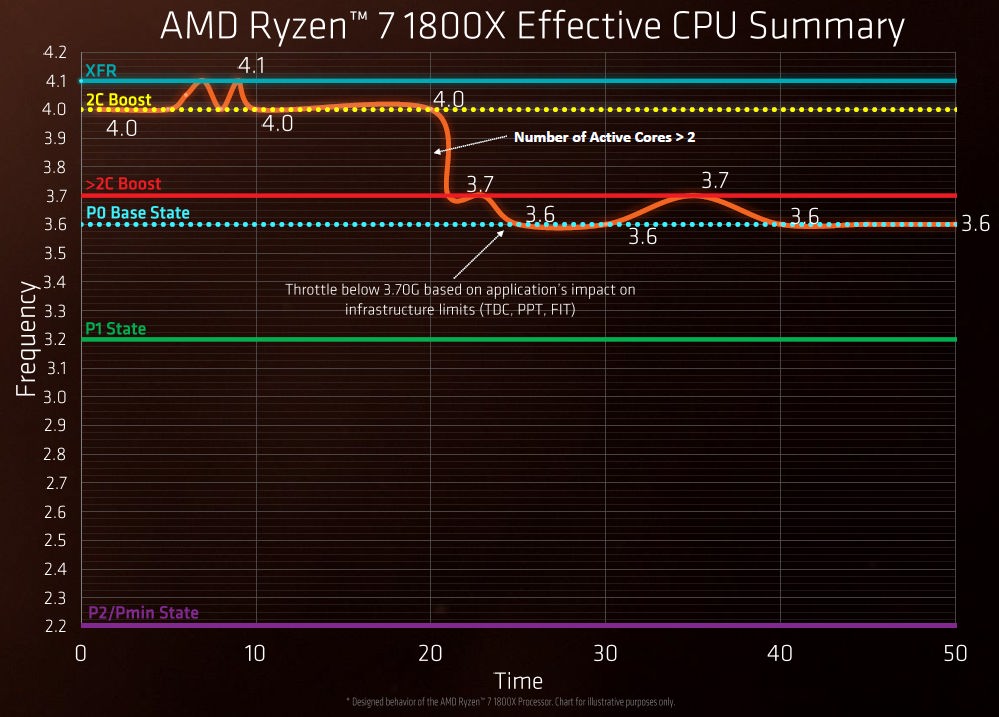
With its 25MHz increments, the Zen clock speed can vary smoothly between its standard clock and its boosted maximum.
Enlarge / With its 25MHz increments, the Zen clock speed can vary smoothly between its standard clock and its boosted maximum.
The counterpart to cutting the voltage as aggressively as possible to maintain a given frequency is pushing the frequency up while not exceeding a given power draw. The same control system that cuts power can also push up the clock speed of each core to make maximum use of the processor’s power budget. This kind of turbo boosting is nothing new, but AMD’s system, “Precision Boost,” has a couple of novel attributes. The first is that the boosting is fine-grained; it can adjust the clock speed in 25MHz increments.
Second, the clock speed can be pushed beyond the standard boosted maximum if the sensors detect that there is still thermal headroom available, which AMD is calling Extended Frequency Range (XFR). If the heatsink and cooler are significantly above the minimum spec and hence the chip is running cool, XFR will add up to 100MHz extra clock speed (for the 1800X and 1700X; it adds only 50MHz to the 1700), in essence giving a tiny overclock “for free.”
These refinements and optimizations to power distribution, timing, and voltage, account for the remaining 70 percent of the performance per watt improvement.
When it comes to “real” overclocking, however, the R7 processors are a mixed bag. On the one hand, they’re all multiplier unlocked, at least when used in conjunction with the right chipset, so you’re free to experiment in whatever way you see fit. AMD estimates that most 1800Xes will manage 4.2GHz across all eight cores, as long as they’re bumped up to 1.45V. AMD also estimates, however, that 1.45V will shorten the life of the chip.
Enabling overclocking mode, however, disables much of the fancy power management. There’s no way, for example, to say that you’d like XFR to add 200MHz of extra speed, subject to thermal constraints. Nor can you, say, set an 1800X to run at a 3.8GHz base, 4.2GHz turbo (bumping both by 200MHz). As soon as overclocking is enabled, the processor simply runs at a fixed speed (when in the P0 power state).
This stands in contrast with Intel, where you can specify the turbo multipliers for 1, 2, 3, and 4-core boosting, and with Kaby Lake, where you can even set a reduced multiplier for use during AVX-intensive workloads. As smart as Zen is in normal operation, it’s very simplistic in overclocked mode.
A platform that includes a chipsetless chipset
The Ryzen R7 is not just a processor; it’s a system-on-chip. Whether it’s used in this capacity, however, will depend on which motherboard and chipset it’s paired with.
The processor itself has 20 PCIe 3.0 lanes, 4 USB 3.1 generation 1 (5 Gb/s) controllers, and a further 4 mixed PCIe and I/O lanes; these can be grouped for a single x4 NVMe device or split into 2 SATA plus 1 x2 NVMe or 2 SATA plus x2 PCIe. There are also two DDR4 memory channels.
Of those 20 PCIe 3.0 lanes, four are normally used to communicate with the chipset. AMD has three regular chipsets; the high-end X370, mid-range B350, and low-end A320. All include USB 3.1 generation 2 (10 Gb/s) controllers (two for the X370 and B350, one for A320), six USB 2 controllers, some additional SATA controllers (4, 2, and 2, for X370, B350, and A320, respectively), two SATA Express ports (which can be used as 4 SATA 3.0 ports), and some PCIe 2.0 lanes (8, 6, and 4). The X370 and B350 both enable overclocking, and the X370 allows the 16 remaining PCIe 3.0 lanes from the processor to be split into 2×8 channels for dual GPU support.
But for small systems, the extra I/O and extra size of a chipset might be undesirable. Accordingly, there are two other chipsets, X300 and A/B300, that greatly diminish what it means to be a chipset. With X300 or A/B300, the only I/O capabilities are those within the processor itself; they don’t include USB 3.1 generation 2, they don’t include SATA Express, they don’t add any PCIe 2.0 lanes. The chipsets provide a handful of functions, mainly around security and provision of a Trusted Platform Module. As such they are tiny: AMD says they’ll fit on a chip the size of a fingernail.
Because these chipsets do so little, they don’t need four PCIe lanes from the processor; there’s a dedicated SPI link for them. This means that all 20 of the processor’s PCIe lanes become available. The X300 also enables overclocking and dual GPUs.
Regardless of chipset, AMD intends to use the same socket, Socket 1331, and the same platform, AM4, until 2020, unless some new technology (such as PCIe 4.0 or DDR5) forces it to change the package pinout. Ryzen AM4 motherboards are compatible with existing AM4 APUs, and they’ll also work with Raven Ridge Zen-based APUs that should become available later this year. This is why pretty much all of the Zen motherboards include integrated display outputs, even though right now, Ryzen processors can’t use them.
AMD’s gambles starting to pay off
It’s already clear that Zen is a tremendously more successful architecture than Bulldozer was. Bulldozer was barely competitive with AMD’s existing products, and it was left in the dust by Intel’s chips. That’s not true of Zen. AMD’s new architecture is performance-competitive with Intel’s Broadwell, and it’s efficient, too.
But the question of whether to buy a Zen is a complex one, and it’s complex for many of the same reasons that Bulldozer was so weak. For highly multithreaded workloads, Zen is much more cost-effective than Broadwell-E, while performing at almost exactly the same level. Sometimes Broadwell-E will be a little faster, sometimes Zen will be a little faster, but with the exception of workloads that are particularly dependent on AVX or memory bandwidth, it’s a wash. That makes AMD’s $499 part an easy and attractive alternative to Intel’s $1,049 chip.
I’d expect developers, for example, to be keen to get their hands on Zen as soon as they can. Software compilation, especially of C++, is readily multithreaded and almost invariably CPU-bound, and doubling the number of cores and threads is a huge performance win. Video game streamers are another demographic that AMD is courting with much the same logic: a chip with lots of cores has the capacity to both play a game and perform high quality video compression, which is something that Intel’s four core parts struggle at.
But in other workloads, Intel’s greater single-threaded performance is the more important factor. In games including Grand Theft Auto V, Battlefield 4, and Ashes of the Singularity, the Kaby Lake i7-7700K will pull ahead of the 1800X in spite of having half the number of cores and threads.
Just as it was with Bulldozer, AMD’s hope is that developers will build their software to scale better onto larger numbers of cores, allowing Zen to more consistently show its benefits over Intel’s chips. But a look at the Steam Hardware Survey illustrates why, in the short term at least, developers might be reluctant to do that; 2- and 4- core processors make up the overwhelming majority of gaming systems.
The big difference, however, is that Zen is still good enough to be competitive even in workloads that aren’t optimal. An i7-7700K may offer slightly higher frame rates and slightly better performance for a particular workload, but where Bulldozer was just downright embarrassing for single-threaded tasks, Zen is still good?good enough that you may well be willing to take the performance hit in some programs so that you can enjoy the big wins in others.
That’s simply not a position that AMD has been in for a long, long time. It’s been many years since PC enthusiasts have had to seriously consider which processor to buy, but AMD has built something that’s absolutely worth consideration. It might not be the right chip for everyone, but this time around, it is at least the right chip for someone.
来源:http://www.ednchina.com/news/article/20170314zen
作者:Peter Bright
原文链接:https://arstechnica.com/gadgets/2017/03/amds-moment-of-zen-finally-an-architecture-that-can-compete/
MIT钱愉盈编译
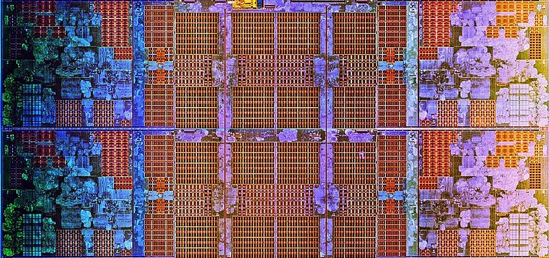


上面关于1500x的描述好像不对吧,1500x应该是两个关闭了两核的ccx,而不是一个ccx_(:3」 ∠)_