【AMD Vega10和Vega20参数曝光:12TFLOP单精度,17年下半年双芯登场】AMD Vega 10 and Vega 20 GPU Details Leak Out ? 12 TFLOPs of Single Precision Compute, Dual GPU Landing in 2H 2017
Our colleagues over at Videocardz.com have posted some very tasty information on the upcoming Vega 10 flagship from Radeon Technologies Group, AMD. This particular leak is very significant, because not only is this the first time we have had concrete numbers on the performance of the upcoming flagship but it also confirms the existence of a dual Vega based graphics card from AMD that is in the works. AMD is expected to introduce its first Vega 10 based flagship sometime in the first half of 2017.
【我们从RTG获取了关于即将到来的Vega10旗舰的消息。这次曝光不仅是我们首次得到确切的各项参数,也是首次确认双芯Vega的存在。AMD预计2017年上半年发布首个采用Vega10的旗舰。】
New information about the Vega 10 and Vega 11 GPUs ? Dual Vega 10 based graphics card inbound
【关于Vega10和Vega11的新消息 – 双芯Vega10研发中】
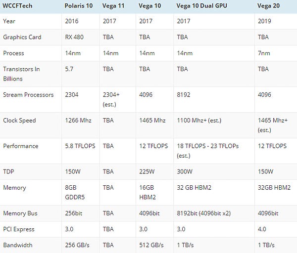
It will contain 64 Compute Units, which (assuming the same ratio of CU to SPs as the current iteration of GCN) translates to exactly 4096 Stream Processors. The internal codename of this GPU is GFX9. Remember all our internal nomenclature analysis? Well, it’s the same thing, only in a more appealing format. Hawaii was GFX7, Polaris is GFX8 and Vega is GFX9.
【Vega10将有64个CU,即4096SP,Vega架构的内部代号为GFX9,Hawaii是GFX7,而Polaris是GFX8。】
The GPU is stated to be manufactured on the 14nm FinFET node which means you are looking at primarily GlobalFoundries based chips here (with Samsung based chips as required under the amended WSA). It will be shipping with 16GB of HBM2 memory, with roughly 512 GB/s of bandwidth (the source states 512 Gbps but I believe that is a typo). The TDP is slated to be around 225W.
【Vega10将由GF的14nm制程打造,配有16GB HBM2显存,带宽512GB/s(来源说是512Gbps,应该是打错了),TDP大概225W】
Here comes the interesting part, however, according to VCZ, the GPU will have roughly 24 TeraFLOPs of 16-bit compute. 16 bit compute is, of course, half-precision work and if Vega has native 16-bit compute support then we can find out the single precision performance by simply cutting the number in half: 12 TeraFLOPs of compute. A solid, concrete number is more than any tech journo can ask for, but it allows us to easily reverse engineer the clock speed the GPU will be clocked at.
【据说Vega10的16bit计算能力能达到24TFLOPs,如果Vega原生支持16bit计算,那么单精度大概就是12TFLOPs,很容易可以反向推出大概的GPU频率。】
With a single precision compute of 12 TeraFLOPs per second on a GPU with 4096 cores, and considering TeraFLOPs is a function of Clock Speed * 2 Instructions Per Clock * Cores, you are looking at a Vega 10 graphics card that is clocked at roughly 1465 Mhz. Considering the Polaris 10 GPU is clocked at 1266 Mhz however, this is a fairly significant step up from the last iteration and probably due to the increasing maturity of the 14nm node over at GlobalFoundries. On the other hand, just in case this information turns out to be inaccurate later on, I can tell you that even if we were assuming a clock rate similar to Polaris 10 (1266 Mhz), you are still looking at a single precision compute of 10.3 TeraFLOPs. Which is still, a huge performance leap over the mainstream-oriented Polaris 10.
【因为Vega10有4096个SP,单精度12T,而TFLOPs计算公式为主频x2(每周期2条指令)x核心数,那么Vega10的主频就是大概1465MHz。要知道P10主频也只有1266MHz,这是一次很大的进步,应该是GF的14nm工艺不断成熟的结果。另一方面,预计也可能不大准确,因为就算主频只有P10的1266MHz,单精度依然能打到10.3TFLOPS,依然比主流的P10高出许多几个华莱士】
So how does this compare to the Nvidia high end? Well, trouble is, we do not know the specs for Nvidia’s GP102 based GPU yet. There had been a leak some time ago, but considering we were fairly sure it was fake, I never published it. However, we do know that it will probably have fewer cores than the P100 but will be clocked higher. A Vega 10 GPU, at both clock rates (1465 Mhz or 1266 Mhz) easily beats out the P100 on paper ? which has a single precision performance of 9.3 TeraFLOPs for PCI-e based cards. It goes without saying that since we are comparing across two completely different architectures here, what is on paper can be different in real life. The ball is now undoubtedly in Nvidia’s court and we shall see what its high-end looks like in the coming months.
【那么和NVIDIA的高端比呢?但是我们现在都不清楚GP102的确切参数,之前的曝光是假的,我就没发出来。我们能确定的是,GP102的CUDA核心数比P100更少,但主频会更高。光一个Vega10 GPU,在1465MHz(或者更加保守的1266MHz)下,纸面数据可以轻松击败P100 – PCIE版的P100的单精度只有9.3TFLOPS。当然,我们这是在比较两个不同架构,纸面数据和实际情况会不同。现在轮到NVIDIA接球了,我们可以期待一下未来几个月高端市场的变化。】
AMD will be replacing the Polaris 10 chip with the Vega 11 GPU sometimes next year. The latter will be based on 14nm FinFET just like the former but should have a higher spec count (since Polaris 10 is already on the 14nm node, it wouldn’t make sense to a new chip otherwise). So all in all, we are looking at a pretty much top to bottom revamp in the Radeon lineup ? something that should really reinvigorate the company’s GPU side which has been lacking lately. I won’t go into a lengthy rant, but the timing of these GPUs is not a co-incidence. By offering brand new graphics cards for the entire customer spectrum AMD is allowing customers to build PCs which are completely red. With Zen releasing as well next year, and the company having already introduced its AM4 motherboards and Memory Sticks, pretty much the only component that won’t be manufactured by AMD will be the casing and the PSU.
【明年AMD将会用Vega11作为Polaris10的换代,Vega11同样基于14nm工艺,SP数量应该会更多(P10已经是14nm了,没有道理去再造一个同样的GPU)。总而言之,Vega将会带来全新的Radeon产品线,大幅提升性能。Vega的发布时间刚好和明年Zen对上,这应该不仅仅只是个巧合,AMD可能会带来全新的3A平台。】
The leak also states that AMD will be releasing a dual-GPU based graphics card later on in the second half of 2017. Knowing AMD, this dual Vega 10 GPU graphics card will probably have the full blown cores at lowered clock rates (TDP is said to be approximately 300W). On paper, and at a rough estimate without any knowledge of clock rates, the card should be capable of 19-22 TeraFLOPs of single-precision compute ? which is an absolutely ginormous amount of graphical horsepower. 4K Eyefinity setups might be coming next year folks.
【曝光还说AMD将会在2017年下半年带来一款双芯Vega10显卡,按照惯例,应该是两颗运行在较低主频的完整的Vega10(TDP大概300W),这张卡的计算能力可能达到19-22TFLOPs – 简直可怕。另外Eyefinity的4K支持也可能在明年到来。】
Vega 20 GPU will be landing on the 7nm node
【Vega20将会使用7nm工艺】
Vega 20 will be building on AMD’s philosophy of curtailing excess and should bring significant leaps in power efficiency and performance per watt. The GPU will have the same core count as the Vega 10 GPU at 64 Compute Units and will be based on the 7nm FinFET architecture. Since the designation remains GFX9, we can easily assume that this is, in fact, a simple node shrink of the Vega 10 GPU ported over to 7nm with bigger and better memory (it will have 32 GB HBM2 with 1 TB/s of bandwidth).
【新的Vega20将会大幅提升能效,规格依然是64CU 4096SP,但将会基于7nm FinFET制程,所以它应该就只是Vega10的制程更新版本,同时升级到32GB HBM2,带宽1TB/s】
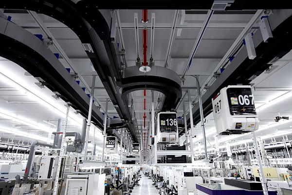
A clean room in Fab 1, GlobalFoundries.
【GF的Fab1】
The graphics card will support the PCI Express 4.0 standard and will have a TDP of 150 Watts. It is possible that the node shrink will allow it to achieve higher clocks resulting in the card effectively beating the Vega 10 not only in terms of performance per watt but in terms of actual graphical horsepower as well.
【Vega20将会支持PCIE4.0规范,TDP150W。新制程下主频会更高,性能和能效都会超越Vega10】
As far as when the time horizon goes, according to foundry roadmaps, you are looking at 7nm landing by 2017 and ready for high-powered ASIC production by 2018. Knowing that foundry schedules are about as solid as the weather, this isn’t anything more than an estimated timeframe, it could easily be more (or less).
【至于它什么时候到来,按照GF路线图,7nm是在2017年【现在已经开始内部测试,下半年接受用户设计】,2018年才能够生产高性能产品。要知道这些个代工厂的路线图基本上和天气一样变幻无常,只会推迟不会提前。】
From what I can gauge from these specifications, the Vega 20 GPU will be able to offer the power of a very high-end GPU at a much more reasonable price (remember, node shrinks bring economies of scale with them!) unless AMD decides to chase margins. The 150 Watt TDP means that it will be able to fit into most power supplies and effectively put serious gaming power in the hands of the mainstream gamer.
【Vega20将会带来高端的性能,同时价格会很合理,除非AMD改变策略去追求利润。150W的TDP也能让大多数的电源带动。】
But what about Navi 10 and 11?
【Navi10和Navi11呢?】
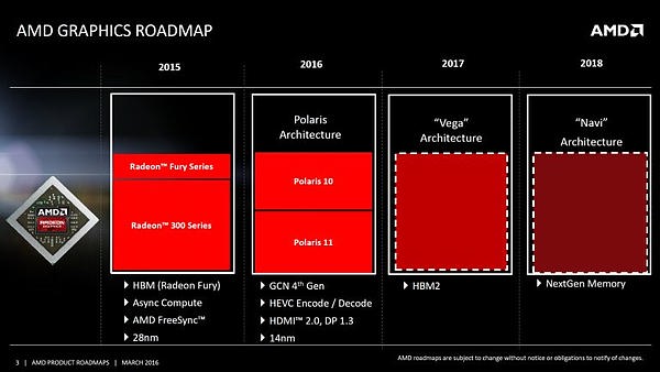
Navi is the next generation architecture (next-next generation?) which will succeed Vega. However, according to this leak, it has been delayed by one year due to the introduction of the new chips in the Vega lineup. It will now be landing sometimes in 2019. Navi 10 and Navi 11 will replace Vega 10 and 11 respectively and should offer a significant upgrade over the former due to an increase in core count. Since the architecture is pretty far out into the horizon, there isn’t much point talking about it right now. That said, however, it is clear that RTG is introducing the Vega 10 based dual-GPU to keep high-end enthusiasts happy till the time Navi arrives ? considering it will probably be able to rock more power than the latter (which is a single chip card).
【Navi是Vega之后下代架构。然而根据爆料,由于Vega产品线中新GPU的引入,它已经推后了一年,将会在2019年到来。Navi10和Navi11会取代Vega10和Vega11,也会带来性能的显著提升。】
AMD Next Generation Vega 10, 11, 20 and Dual GPU Graphics Card Lineup
【AMD下代 Vega10/11/20/双芯产品线】
source:http://wccftech.com/amd-vega-10-vega-20-gpu-details-dual-graphics-card/
自翻,转载请注明出处,严禁私自篡改标题、内容以及二次投递。
