source:http://videocardz.com/63450/amd-vega-to-launch-in-1h-2017
自翻,转载请注明出处,严禁私自篡改标题、内容以及二次投递。
This is the latest information coming directly from AMD about VEGA architecture. Apparently the rumors that the launch of VEGA architecture might have been pushed forward were not entirely correct.
【这是AMD VEGA架构的最新直接消息。很显然之前VEGA提前发布的传言并不完全正确。】
AMD VEGA in 2017【VEGA 2017年发布】
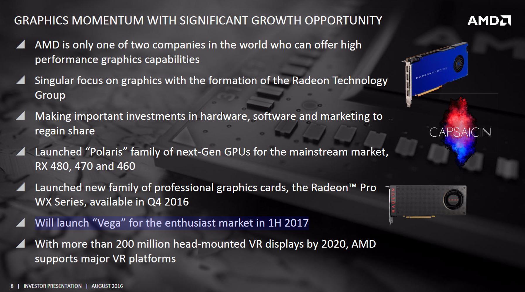
You can find the following slides in the latest presentation for AMD investors. Those slide confirm that VEGA will not launch sooner than first half of 2017, so just as expected after first roadmaps were released. It’a also worth adding that this preliminary date may still change, as explained in the footnotes of the document:
【从AMD展示给投资者的ppt中可以找到以下信息 – VEGA最早也是2017年上半年发布,和刚发布路线图时预料的一样。但也要指出一点:这个大致时间也可能会改动,因为文档的注脚写着:】
The information contained herein is subject to change and may be rendered inaccurate for many reasons, including but not limited to product and roadmap changes,【文档所含信息(包括但并不限于产品和路线图变动)可能会改动,由于各种原因,可能并不准确。】

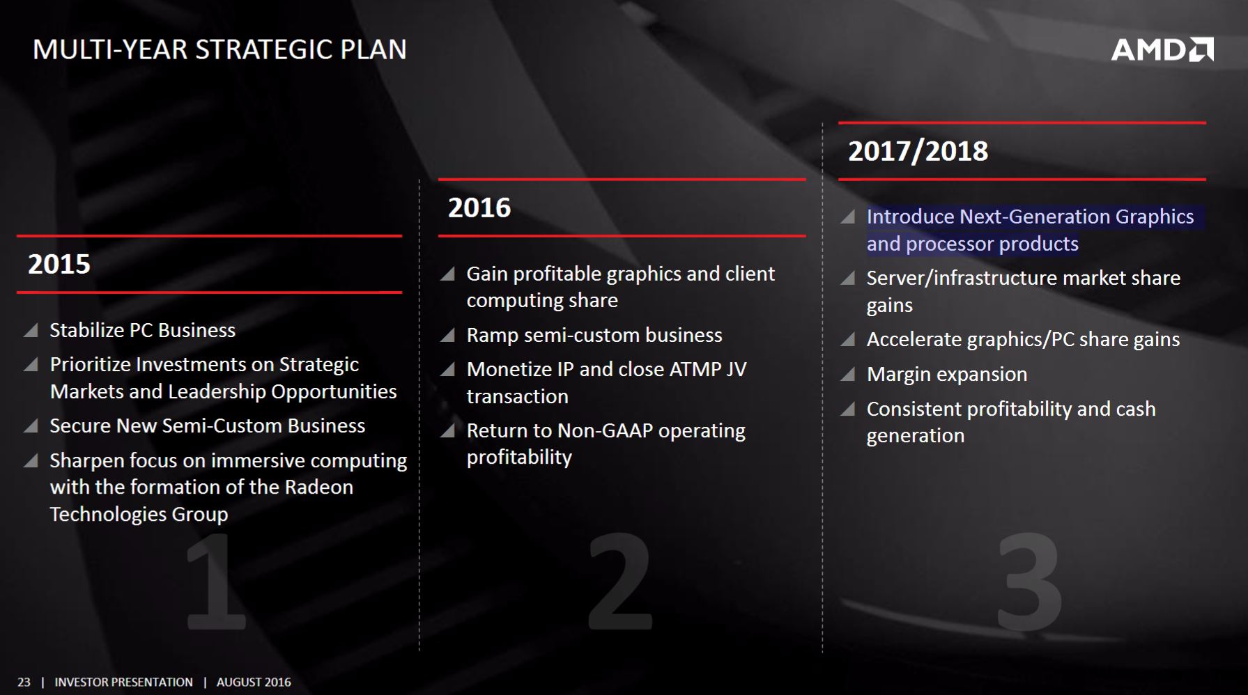
AMD is planning to introduce next-generation graphics in the following years. This means Vega and probably Navi architecture coming in 2018.
【AMD准备明年引入下代显卡- VEGA,Navi架构可能在2018年。】

Teasers from AMD【来自AMD的预热】
Just two weeks ago Chris Hook (Sr. Director, Global Marketing and PR at AMD) posted this picture showing ‘Vega launch venue’.
【两周前Chirs Hook(AMD全球市场与公关高级总监)发了张“Vega发布会场”的照片】

Two months ago Raja Koduri (Sr. Vice President and Chief Architect at RTG) was celebrating, with a group of engineers, Vega 10 reaching a development milestone. It could mean that that the final design of Vega 10 has been accepted and it should take few months for actual GPU to be seen on the market.
【两个月前Raja Koduri(RTG的高级副总裁和主架构师)和一群工程师庆祝Vega10研发达到了一个里程碑。这可能意味着Vega10的最终设计拍板,实际的GPU进入市场还需好几个月。】

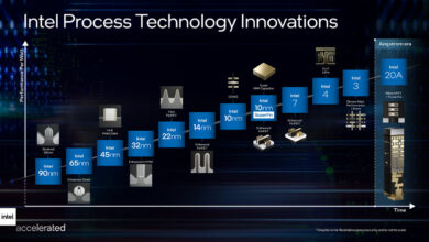
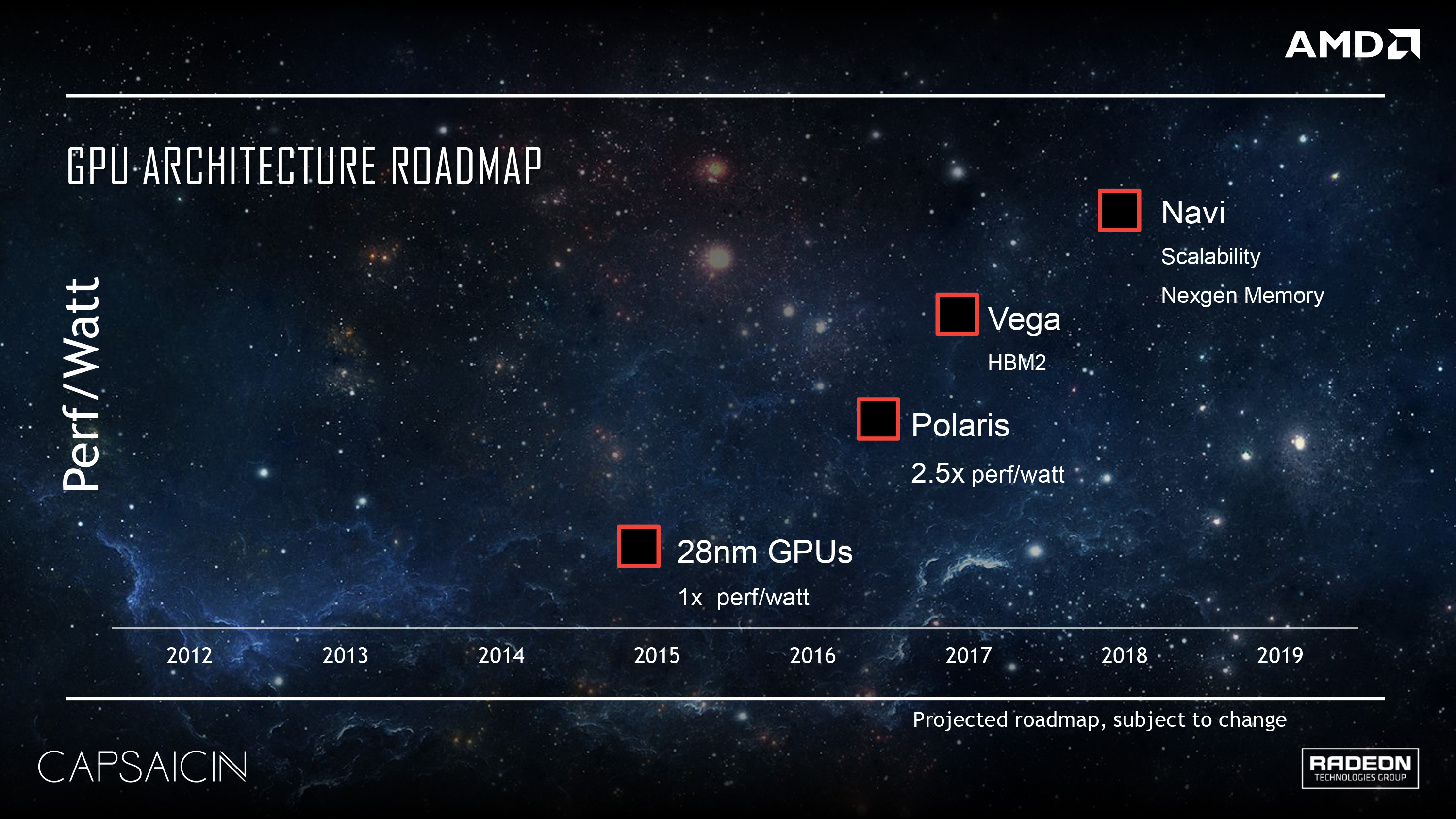
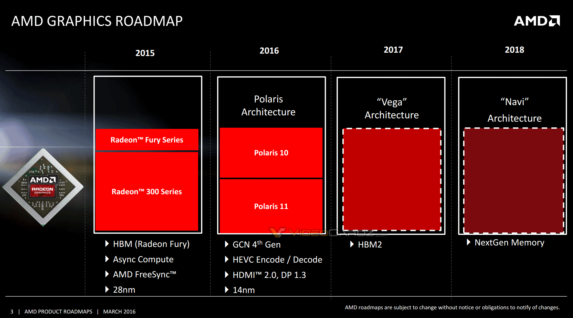
In March AMD has released two roadmaps. We learned that Vega will use High-Bandwidth-Memory Gen2 and, in a very optimistic scenario, it should be around 3x more power efficient than 28nm GPUs. Optimistic, because the same slide said 2.5x perf/watt for Polaris, which has since then been changed to 2x perf/watt in newer materials (including investors presentation from this post).
【三月份AMD发布了两张路线图。Vega会使用HBM2,乐观的情况下会比28nm GPU能耗比高3倍。为什么说“乐观的”?因为这张PPT上Polaris的2.5倍能耗改善在新ppt中改成了2倍。】

