【AMD Radeon RX 480 架构预览:Polaris赢得了主流市场】The AMD Radeon RX 480 Preview: Polaris Makes Its Mainstream Mark
source:http://www.anandtech.com/show/10446/the-amd-radeon-rx-480-preview
本文主要是对Polaris的改进进行了简单介绍,以及部分游戏测试,但游戏测试与tom’s hardware上差距较大(驱动尚存bug),还是等正式测试再做观察
由于是Preview,更全面的Review过几天就会出,所以就不逐字逐句翻译了,选重要的架构信息翻译一下好了…(懒

Back in December of last year, AMD’s Radeon Technologies Group began slowly trickling out the plans for what would be their first GPU architecture built for the now-modern FinFET processes: Polaris. As part of a broader change in how GPU architectures have been handled ? more information is now released ahead of launch ? AMD laid out what they wanted to do with Polaris. Aim for the mainstream, radically improve power efficiency, lay the groundwork for HDR displays, and, of course, improve performance.
Now six months later we are seeing AMD’s plans come to fruition, as the Polaris GPUs are in full production, and the first retail products are launching today. Kicking off the Polaris generation in the desktop market will be AMD’s Radeon RX 480, which is aiming for the mainstream market. We’ve already seen the card, the price, and AMD’s marketing spiel back at Computex 2016, so now it’s time to take a look at the final, retail hardware.

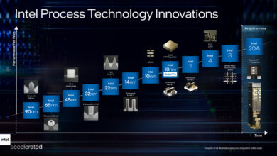
At the highest level, the RX 480 is based off of a fully enabled version of AMD’s Polaris 10 GPU. This is the first Polaris GPU to hit the market, and is the larger of the two GPUs. The total transistor count is 5.7 billion, which takes up 232mm2 on GlobalFoundries’ 14nm FinFET process. That this GPU is built at GloFo and not TSMC is a significant departure for AMD, who previously has used partner TSMC just shy of forever, and is the first time AMD and NVIDIA haven’t used the same fab in some 13 years. We’ll touch upon the foundry issue more in the full review, but the important thing to take away right now is that with the split in foundries, it’s no longer architecture alone that dictates whether a given NVIDIA or AMD GPU is better; process now plays a part, and the playing field is no longer even.【更换代工厂后,13年来NV AMD共同使用TSMC的历史结束了,以后代工厂工艺差距也需要纳入考量,而不单纯仅仅只是架构差距】
As it’s using a full Polaris 10 GPU, the RX 480 ships with all 36 CUs (2304 SPs) enabled. Ignoring architectural efficiency for the moment, this puts it somewhere between the Radeon R9 390 (Hawaii) and Radeon R9 380 (Tonga) in terms of CU count, with AMD having spent a good chunk of their 14nm density gains on adding CUs. Note that the CUs themselves have not substantially changed ? it’s still 64 stream processors and 4 texture units per CU ? which is where the 144 texture unit counts comes from.【光看CU数量,定位在R9 390和R9 380之间,144个TMU】

On the backend of things, RX 480 is equipped with 32 ROPs. This is fewer than Hawaii’s 64 ROPs, but it is consistent with mainstream parts, as ROP needs don’t scale nearly as quickly from one generation to the next like compute (CU) needs. These 32 ROPs are paired with 2MB of L2 cache, which is twice as much L2 cache per ROP as the bulk of AMD’s last-gen lineup. The increased L2 cache has a die space cost ? which is now easier to pay with the 14nm process ? and helps to improve performance and cut power consumption by keeping more data on-die.【后段32ROP,比Hawaii的64ROP砍半,搭配2M L2,相对于GCN1.2翻倍】
However once you go off-die, you will run into RX 480’s VRAM, which is a small story in and of itself. Once again common for mainstream AMD cards, AMD has stuck with a 256-bit GDDR5 memory bus here. Attached to this bus is either 4GB or 8GB of VRAM, with AMD offering two capacities for RX 480. The reason for offering multiple capacities is that AMD wants to hit the $199 price point with the card ? the traditional sweet spot for mainstream cards ? which would be hard to do with an 8GB card at this time. By offering both, AMD can hit that price while offering a full 8GB card at a slightly higher price for buyers with a bit more flexibility and/or greater VRAM needs.
Where things get tricky here however is the memory speeds. Officially, 7Gbps GDDR5 is the minimum speed for both RX 480 capacities, and this is the speed that AMD’s 4GB reference card runs at. However for their 8GB reference card, AMD has opted to ship the card with faster 8Gbps memory in order to further boost performance. I suspect that AMD would have liked to have used 8Gbps memory throughout, but the aforementioned price target required AMD to make some concessions to comfortably reach it. Otherwise for the higher priced 8GB card, AMD didn’t need to pinch pennies, and as a result they were able to ship it with 8Gbps memory.【4G/8G版 8G公版显存频率8Gbps,4G为7Gbps,480显存频率要求的最低限是7Gbps,AMD的8GB公版全都是8Gbp显存】

The end result is that we have an odd schism between AMD’s card requirements and what they actually ship. The reference 4GB RX 480 meets the RX 480 minimum specifications, whereas the reference 8GB card is de facto overclocked relative to those same specifications. As we’ll see in our benchmark results, the difference in performance isn’t too great, but I don’t think this is an ideal outcome for consumers. My biggest concern right now is what happens when AMD’s partners start shipping their custom cards; if they opt for slower memory buses, then this would mean that custom 8GB cards could end up slightly underperforming the official reference card. But we’ll have to see how that plays out.【如果AIB选择为8GB版搭配7Gbps显存,那么会出现非公不如公版的情况】
Moving on, let’s talk about power consumption. As AMD has made clear over the last several months, one of the major goals of Polaris was power efficiency, and this is where we see some of the first payoffs from that decision. RX 480’s official Typical Board Power (TBP) is 150W, over 20% lower than the last-generation R9 380, and 45% lower than the otherwise performance-comparable R9 390. Consequently the card only requires a single 6-pin PCIe power connector for external power, making it a more friendly option for power-limited desktops that don’t offer additional power connectors.
【大部分供电为单6pin】

In terms of design, the reference RX 480 is a double-wide, blower-style card measuring 9.5-inches long. Notably, this is the first AMD retail reference card since the Radeon R9 290 series to use a blower, giving AMD the opportunity to show that they’ve learned from 290’s excesses and that the company can build a better blower. Given AMD’s mainstream ambitions, a blower makes a lot of sense for a $199, 150W card, as a fully exhausting card is going to be the most compatible with the wide variety of desktop designs out there. AMD doesn’t need to worry about whether the cooling built into the chassis can handle 150W of heat, since the card can remove the vast majority of the heat on its own. The blower design does add some length to the card though; the PCB is only 7-inches long, while the space requirements for the radial fan push the card out to the full 9.5-inches.
For connectivity, buyers will find 3 DisplayPorts and an HDMI port; AMD has done away with the DVI port for their reference design. As this is a new card on a new architecture, both port types support their latest respective standards. For DisplayPort this means support for the 1.3 and 1.4 standards, adding the newest, fastest HBR3 signaling mode, along with full HDR support. Meanwhile for the HDMI support, HDMI 2.0b is supported, offering 4Kp60 support with HDR.【接口为3DP 1HDMI 公版去除了DVI,DP接口支持1.3 1.4标准,HDMI支持HDMI2.0b标准,可以满足4K 60FPS+HDR】
For today’s launch, this is going to be a full reference launch. All of AMD’s partners are shipping AMD’s reference design in 4GB and 8GB capacities, which means the differences between the vendors will come down to pack-in items, support, and whether anyone charges a premium for the aforementioned items. Card availability is said to be good, but at this point I’m going to be surprised if most retailers don’t sell out by the end of the day, as these days it’s rare for video cards not to sell out, even mainstream cards. Looking at the slightly longer term, AMD isn’t able to state exactly when we’ll see custom RX 480 boards hit the market, but from what I gather it will be sooner rather than later.
Moving on, with two different capacities there are two different prices for the RX 480. The entry level 4GB card will be launching at the previously unveiled price of $199. Meanwhile the 8GB card will launch at $239, a $40 price premium for the extra 4GB of memory and the higher memory frequency. I do not have a good idea of what the split is between 4GB and 8GB cards, but I suspect that it will be the 8GB cards that are more plentiful.
Finally, looking at the competitive landscape, just as was the case last month with NVIDIA’s GTX 1000 series and the high-end market, the Radeon RX 480 series is launching uncontested into the mainstream market. At least for the time being all of NVIDIA’s products are positioned well above the RX 480 ? with GTX 1070 starting at $399 ? which means what competition there is for AMD is composed of last-generation 28nm cards, particularly the GTX 970 and GTX 960. As these are last-generation cards, neither one is strictly comparable to the RX 480, and in the long run these cards have a limited shelf life as they’re due to be discontinued sooner than later.【RX480的对手是上代的970 960】

AMD’s Path to Polaris
With the benefit of hindsight, I think in reflection that the 28nm generation started out better for AMD than it ended. The first Graphics Core Next card, Radeon HD 7970, had the advantage of launching more than a quarter before NVIDIA’s competing Kepler cards. And while AMD trailed in power efficiency from the start, at least for a time there they could compete for the top spot in the market with products such as the Radeon HD 7970 GHz Edition, before NVIDIA rolled out their largest Kepler GPUs.【7970在Kepler之前发布,抢占了能耗比的先机】
However I think where things really went off of the rails for AMD was mid-cycle, in 2014, when NVIDIA unveiled the Maxwell architecture. Kepler was good, but Maxwell was great; NVIDIA further improved their architectural and energy efficiency (at times immensely so), and this put AMD on the back foot for the rest of the generation. AMD had performant parts from the bottom R7 360 right up to the top Fury X, but they were never in a position to catch Maxwell’s efficiency, a quality that proved to resonate with both reviewers and gamers.【但在中期NV发布了Maxwell,Kepler虽好,但Maxwell做到了非常棒。NV大大改进了架构和能效,使得AMD在后来一直处于下风。AMD一直有足够性能的产品,但能耗比从来没追上Maxwell,这一点大家都心知肚明。】

The lessons of the 28nm generation were not lost on AMD. Graphics Core Next was a solid architecture and opened the door to AMD in a number of ways, but the Radeon brand does not exist in a vacuum, and it needs to compete with the more successful NVIDIA. At the same time AMD is nothing if not scrappy, and they can surprise us when we least expect it. But sometimes the only way to learn is the hard way, and for AMD I think the latter half of the 28nm generation was for the Radeon Technologies Group learning the hard way.【Radeon Technologies Group在28nm后期尝到了GCN能效不足的苦果】
So what lessons did AMD learn for Polaris? First and foremost, power efficiency matters. It matters quite a lot in fact. Every vendor ? be it AMD, Intel, or NVIDIA ? will play up their strongest attributes. But power efficiency caught on with consumers, more so than any other “feature” in the 28nm generation. Though its importance in the desktop market is forum argument fodder to this day, power efficiency and overall performance are two sides of the same coin. There are practical limits for how much power can be dissipated in different card form factors, so the greater the efficiency, the greater the performance at a specific form factor. This aspect is even more important in the notebook space, where GPUs are at the mercy of limited cooling and there is a hard ceiling on heat dissipation.【AMD了解到,比起其他特性,能效更加重要。在笔记本上更是如此。】

As a result a significant amount of the work that has gone into Polaris has been into improving power efficiency. To be blunt, AMD has to be able to better compete with NVIDIA here, but AMD’s position is more nuanced than simply beating NVIDIA. AMD largely missed the boat on notebooks in the last generation, and they don’t want to repeat their mistakes. At the same time, starting now with an energy efficient architecture means that when they scale up and scale out with bigger and faster chips, they have a solid base to work from, and ultimately, more chances to achieve better performance.
The other lesson AMD learned for Polaris is that market share matters. This is not an end-user problem ? AMD’s market share doesn’t change the performance or value of their cards ? but we can’t talk about what led to Polaris without addressing it. AMD’s share of the consumer GPU market is about as low as it ever has been; this translates not only into weaker sales, but it undermines AMD’s position as a whole. Consumers are more likely to buy what’s safe, and OEMs aren’t much different, never mind the psychological aspects of the bandwagon effect.【AMD学到的另一点是,市场占有率的重要性。目前AMD GPU的市占率达到了史上最低点。由于心理上的跟风效应,消费者更倾向于买更加保险的产品,OEM也差不多。】
Consequently, with Polaris AMD made the decision to start with the mainstream market and then work up from there, a significant departure from the traditional top-down GPU rollouts. This means developing chips like Polaris 10 and 11 first, targeting mainstream desktops and laptops, and letting the larger enthusiast class GPUs follow. The potential payoff for AMD here is that this is the opposite of what NVIDIA has done, and that means AMD gets to go after the high volume mainstream market first while NVIDIA builds down. Should everything go according to plan, then this gives AMD the opportunity to grow out their market share, and ultimately shore up their business.
As we dive into Polaris, its abilities, and its performance, it’s these two lessons we’ll see crop up time and time again, as these were some of the guiding lessons in Polaris’s design. AMD has taken the lessons of the 28nm generation to heart and have crafted a plan to move forward with the FinFET generation, charting a different, and hopefully more successful path.
Though with this talk of energy efficiency and mainstream GPUs, let’s be clear here: this isn’t AMD’s small die strategy reborn. AMD has already announced their Vega architecture, which will follow up on the work done by Polaris. Though not explicitly stated by AMD, it has been strongly hinted at that these are the higher performance chips that in past generations we’d see AMD launch with first, offering performance features such as HBM2. AMD will have to live with the fact that for the near future they have no shot at the performance crown ? and the halo effect that comes with it ? but with any luck, it will put AMD in a better position to strike at the high-end market once Vega’s time does come.

The Polaris Architecture: In Brief
For today’s preview I’m going to quickly hit the highlights of the Polaris architecture.
In their announcement of the architecture this year, AMD laid out a basic overview of what components of the GPU would see major updates with Polaris. Polaris is not a complete overhaul of past AMD designs, but AMD has combined targeted performance upgrades with a chip-wide energy efficiency upgrade. As a result Polaris is a mix of old and new, and a lot more efficient in the process.

At its heart, Polaris is based on AMD’s 4th generation Graphics Core Next architecture (GCN 4). GCN 4 is not significantly different than GCN 1.2 (Tonga/Fiji), and in fact GCN 4’s ISA is identical to that of GCN 1.2’s. So everything we see here today comes not from broad, architectural changes, but from low-level microarchitectural changes that improve how instructions execute under the hood.
【Polaris采用的GCN4相对于GCN1.2来说没有很大改变,实际上GCN4的ISA与GCN1.2完全相同。所以今天我们看到的这些不是大的架构改动,而是从底层微架构层面的改动,来改善指令执行情况】

Overall AMD is claiming that GCN 4 (via RX 480) offers a 15% improvement in shader efficiency over GCN 1.1 (R9 290). This comes from two changes; instruction prefetching and a larger instruction buffer. In the case of the former, GCN 4 can, with the driver’s assistance, attempt to pre-fetch future instructions, something GCN 1.x could not do. When done correctly, this reduces/eliminates the need for a wave to stall to wait on an instruction fetch, keeping the CU fed and active more often. Meanwhile the per-wave instruction buffer (which is separate from the register file) has been increased from 12 DWORDs to 16 DWORDs, allowing more instructions to be buffered and, according to AMD, improving single-threaded performance.
【AMD声称GCN4在GCN1.1(R9 290)基础上单CU性能提升15%。这个是两个重大改变:指令预取和更大的指令缓存 带来的。GCN4可以在驱动帮助下实现指令预取,而GCN1.X不能。这提高了CU的利用率。另外每wave的指令缓存(与寄存器隔离)也从12DWORDs提升到16DWORDs】
Outside of the shader cores themselves, AMD has also made enhancements to the graphics front-end for Polaris. AMD’s latest architecture integrates what AMD calls a Primative Discard Accelerator. True to its name, the job of the discard accelerator is to remove (cull) triangles that are too small to be used, and to do so early enough in the rendering pipeline that the rest of the GPU is spared from having to deal with these unnecessary triangles. Degenerate triangles are culled before they even hit the vertex shader, while small triangles culled a bit later, after the vertex shader but before they hit the rasterizer. There’s no visual quality impact to this (only triangles that can’t be seen/rendered are culled), and as claimed by AMD, the benefits of the discard accelerator increase with MSAA levels, as MSAA otherwise exacerbates the small triangle problem.
【AMD也加强了前端,增加了Primative Discard Accelerator,在渲染管线前,甚至是到达顶点渲染器之前,就能够去除无用(无法渲染/不可见)的部分多边形,声称MSAA开的越高,带来的提升就越高,因为正是MSAA加重了这种无用多边形给GPU带来的负担。】

Along these lines, Polaris also implements a new index cache, again meant to improve geometry performance. The index cache is designed specifically to accelerate geometry instancing performance, allowing small instanced geometry to stay close by in the cache, avoiding the power and bandwidth costs of shuffling this data around to other caches and VRAM.
【增加了地址缓存】
Finally, at the back-end of the GPU, the ROP/L2/Memory controller partitions have also received their own updates. Chief among these is that Polaris implements the next generation of AMD’s delta color compression technology, which uses pattern matching to reduce the size and resulting memory bandwidth needs of frame buffers and render targets. As a result of this compression, color compression results in a de facto increase in available memory bandwidth and decrease in power consumption, at least so long as buffer is compressible. With Polaris, AMD supports a larger pattern library to better compress more buffers more often, improving on GCN 1.2 color compression by around 17%.
【ROP/L2/内存控制器也有更新,还带来了新的Delta色彩压缩技术。色彩压缩在GCN1.2基础上提升了17%】

Otherwise we’ve already covered the increased L2 cache size, which is now at 2MB. Paired with this is AMD’s latest generation memory controller, which can now officially go to 8Gbps, and even a bit more than that when oveclocking.
【之前说过L2被翻倍到2MB,以及最新的内存控制器】