【内存的未来:低成本HBM,HBM3,以及DDR5】SK Hynix and Samsung Talk HBM at Hot Chips 28 ? Low Cost HBM, HBM2 and HBM3 In The Roadmap
source:http://wccftech.com/sk-hynix-samsung-micron-hbm-hmc-ddr5-hot-chips/
本译文未经许可不得转载,严禁私自篡改标题、内容以及二次投递。
被盗帖之后,以后的文章都会像这样注明了。
The semiconductor industry has witnessed a massive departure from the conventional technologies in the last few years. The emergence of new memory standards, SOC architecture has paved the way for modern designs for upcoming products. High-Bandwidth memory or HBM might have first arrived in a graphics products but the potential to be part of a bigger ecosystem.
【近几年,半导体业界见证了对传统技术的各种巨大变革。比如新内存标准的出现、走向现代化设计的SOC架构等等。虽然高带宽内存HBM已经来到了显卡产品上,但还有更大的潜在市场。】
SK Hynix and Samsung Discuss HBM Roadmap ? HBM3 and Low Cost HBM Under Development
【SK海力士和三星讨论HBM路线图 – 正在开发HBM3、低成本HBM】
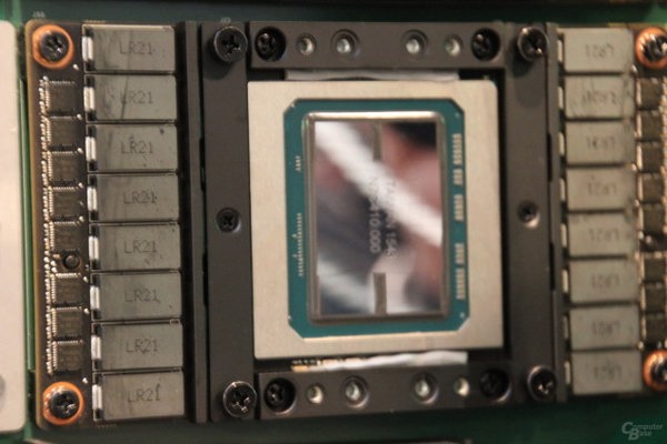
In 2015, AMD unveiled their Radeon R9 Fury X graphics card. The product was the first to feature SK Hynix HBM memory. Delivering up to 512 GB/s bandwidth which was unmatched by any other graphics card in the market. A year later, Samsung ramped up volume production of their own HBM2 DRAM which went on to become part of NVIDIA’s Tesla P100 Hyperscale chip. The super computing chip has been shipping to HPC and Cloud data PCs since Q2 2016.
【去年,AMD发布了Fury X系列,是第一个配有SK海力士的HBM的产品。HBM带来的512GB/s的带宽无人能及。一年后,三星开始大量生产自己的HBM2,后来就用在了NVIDIA的Tesla P100上。从今年第二季度开始P100就已经向HPC和云计算用户出货。】
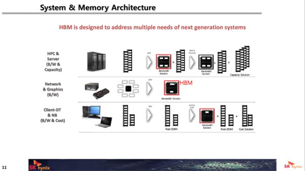
While conventional DRAM model such as GDDR5 are still the go-to-solution for many high-end cards, the future belongs to HBM. Not only is HBM faster, but its also more efficient. This means that it consumes less power and provides higher performance. Another advantage of HBM is that it doesn’t require a lot of space alongside the host chip (CPU or GPU). But since HBM2 is new, it comes at a higher cost and being new also means that overall quantity of the chips being produced is not enough to carter a broad audience of consumers.
【虽然GDDR5这样的传统DRAM依然是很多高端显卡的必备,未来是属于HBM的。不仅因为它更快,更因为它的高能效。因为它能耗更低,性能还更好。HBM的另一个优势是不会在主芯片(CPU/GPU)周围占太多面积。由于HBM2属于新技术,价格现在还很高,产量也不是很充足,不能够满足大量的消费者。】
Samsung initiated production for HBM2 memory back in Q1 2016 while SK Hynix plans to begin production for their HBM2 chips this quarter. At Hot Chips 28, both companies brought forward their catalogs for HBM2 and future roadmaps for HBM.
【三星在今年第一季度开始了HBM2的生产,而海力士是这个季度才开始的。】
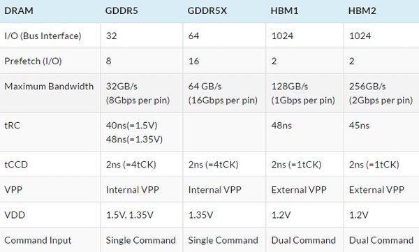
HBM2 Specifications Comparison:
【HBM2参数对比】
Low Cost HBM ? Faster and Cheaper Than HBM1, Built For The Mass Market
【低成本HBM – 比HBM1更快更便宜,为主流市场打造】
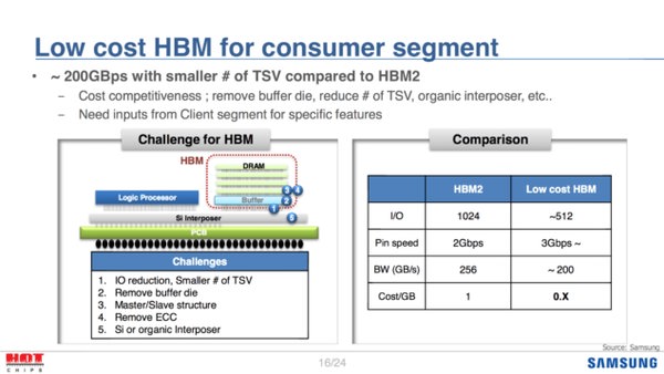
So there are at least two solutions in the works after HBM2, HBMx (HBM3) and low cost HBM. The low cost HBM solution is presented by Samsung and is explained to be more cost effective. It is faster than HBM1 but slower than HBM2 however, it’s supposed to be significantly cheaper. Comparing both HBM2 and HBM (low cost), it is seen that the latter comes with lesser TSVs. TSV standards for through silicon vias which are used to handle the I/O on the DRAM die. The number is reduced from 1024 on an HBM2 stack to 512 on a low cost stack.
【在HBM2之后的下代内存会有至少两种:HBMx(可能为HBM3)和低成本HBM。低成本HBM是三星的技术,在价格上更友好。它比HBM1更快,比HBM2慢,但价格大大降低。对比一下的话,低成本HBM的TSV更少,从HBM2上的1024砍到了512。TSV硅穿孔标准用于DRAM上的I/O处理。】
The end result is a faster pin speed of 3 GB/s (+) that can deliver 200 GB/s compared to 256 GB/s on HBM2. The lower 512-bit interface across 2 / 4 stacks would equate to 1024 / 2048. Samsung believes that they can easily produce these chips in larger quantity and ship it to a mass market.
【在低成本HBM上针脚速度达到了更快的3Gbps以上,可以提供200GB/s的带宽,同等规格的HBM2为256GB/s。虽然基础只有512bit位宽,堆2/4层堆栈,也能达到1024/2048bit。三星有信心大量生产低成本HBM,带到主流市场。】
xHBM or HBM3 ? The Next Generation of High-Bandwidth Memory Chips
【xHBM / HBM3 – 下代高带宽内存】
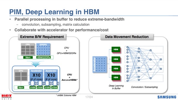
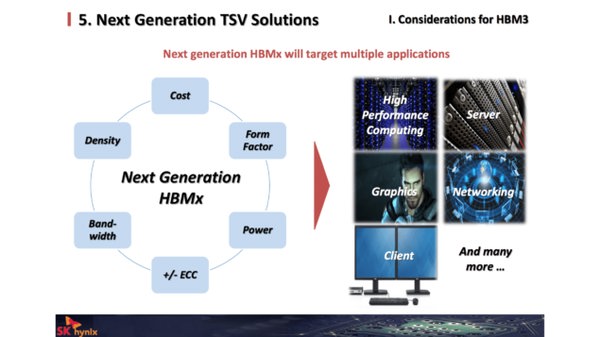
With HBM2 hitting production, SK Hynix and Samsung are already prepping up for the next iteration of HBM memory as demand for bandwidth and efficiency is ever increasing. SK Hynix terms their next solution as HBM3 or HBMx while Samsung calls it xHBM or Extreme HBM.
【随着HBM2的投产,SK海力士和三星已经开始准备下代HBM以应对日益增长的带宽和能效需求。SK海力士称之为HBM3,而三星称之为xHBM(Extreme HBM)。】
The specifications for HBM3 have not been finalized yet and are mostly under consideration at this moment. But two key points that were discussed during Hot Chips and highlighted by Computerbase reveal that HBM3 would offer twice the bandwidth and feature a very attractive price. We are talking about 512 GB/s bandwidth from these chips compared to 256 GB/s offered on HBM2. Four of these stacks would result in over 2 TB/s of bandwidth. Sounds juicy but we sure don’t expect a mainstream graphics card getting that any time soon. May be after Volta?
【HBM3的规格还没定下来,但在这次会议上有消息声称HBM3将带来双倍带宽,价格也会非常有吸引力。HBM2上只有256GB/s,而HBM3会是512GB/s,堆栈4层就能达到2TB/s以上。虽然听起来很棒,但这种玩意肯定不会在主流显卡上马上用上。可能Volta的下代会用?】
Some points in consideration for the next-gen HBM are cost-effectiveness, form factors, power, density and bandwidth. Currently, HBM2 can go as high as 48 GB in terms of capacity so probably expect around 64 GB when HBM3 arrives.
【需要考虑的还有成本、设计、功耗、存储密度和带宽。当前的HBM2的容量最高可以达到48GB,HBM3可能会达到64GB。】
Micron Also Brings DRAM Talk To The Table ? Plans DDR5 For 2019, Calls HBM a Bad Attempt of HMC
【镁光也带来了DRAM – 预计2019年生产DDR5,声称HBM是HMC的劣化山寨版】
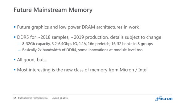
There’s a boom in the DRAM industry these days, Micron also discussed their future roadmaps for DRAM tech at Hot Chips. The company revealed that they plan to sample DDR5 DRAM in 2018 followed by production in 2019. They key purpose behind DDR5 DRAM is to bring twice the bandwidth at just 1.1V. This would mean an increase in clock speeds, capacities would stick to 8 ? 32 GB. Rated frequencies for DDR5 memory would be at 3200 MHz in the beginning and DDR5-6400 MHz when production and yields catch up.
【近些年DRAM产业突飞猛进,镁光也带来了未来的DRAM技术路线图。他们准备2018年准备好DDR5的样品,2019年投产。DDR5的关键提升在于,它能提供DDR4两倍的带宽,而工作电压仅为1.1V。这意味着只有频率提升,而容量还会卡在8-32GB上。刚开始DDR5的等效频率会在3200MHz左右,等到良品率上去之后会达到6400MHz。】
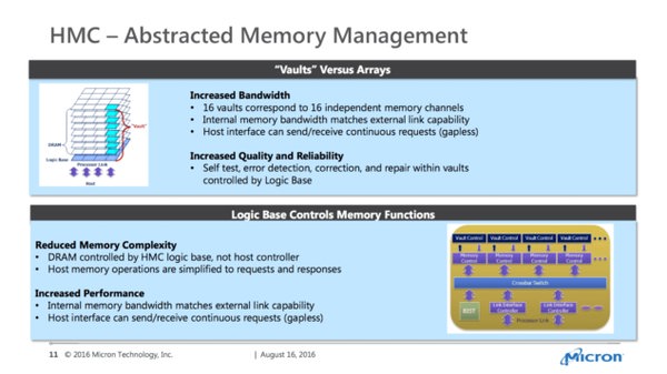
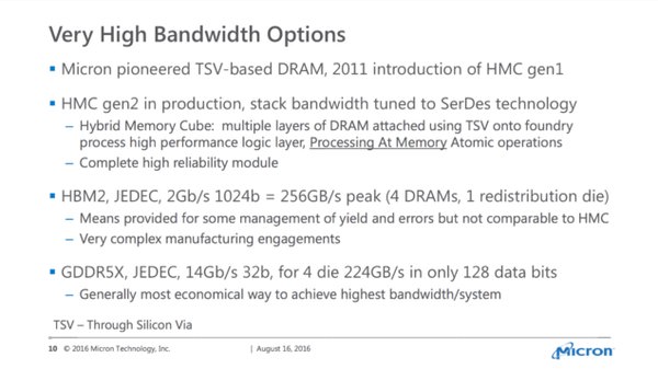
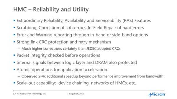
Micron also talked about their high-bandwidth solution known as HMC (Hybrid Memory Cube). The company calls HBM a bad copy of HMC since it has many features that HBM cannot offer outside of bandwidth. Micron also worked on GDDR5X solution which entered the market with NVIDIA’s Pascal based cards and is actively working with Intel on prepping the next generation 3D XPoint memory. You can learn more about that here. There’s definitely a lot of buzz surrounding different memory architectures these days. HBM, HMC and DDR5 are going to be a real deal changer once we approach 2019.
【镁光也谈到了他们的高带宽内存解决方案 – HMC(混合内存立方)。镁光说HBM抄袭HMC抄的很失败,因为HMC除了带宽之外,还有很多HBM不具有的特性。镁光也在开发GDDR5X,它已经随着NVIDIA的Pascal显卡进入市场。镁光还联合Intel开发下代3D XPoint内存。HBM、HMC、DDR5…..听到这么多新架构,现在你肯定很晕。但到了2019年,它们将带来真正的变革。】
请支持独立网站,转发请注明本文链接:http://www.moepc.net/?post=389
雖然說得HMC很牛逼,可是micron的DDR4就是個垃圾?