【AMD下代X86 Zen详细信息】AMD Summit Ridge Processor With Zen CPU Architecture Shown off ? 8 Core / 16 Thread Enthusiast Chip For AM4 Desktop Platform
source:http://wccftech.com/amd-zen-summit-ridge-fx-processor/
自主翻译,转载请注明出处。
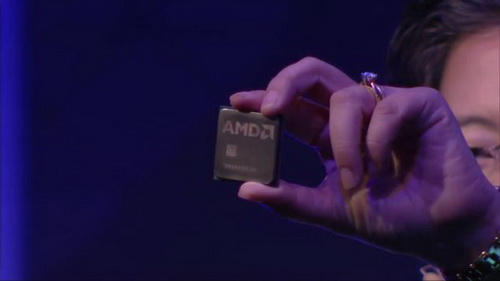
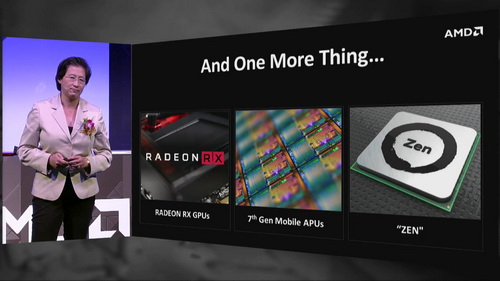
AMD’s CEO, Lisa Su, has just shown off the first sample of their company’s Zen architecture based Summit Ridge processor. The latest chip was shown off to several members of the press at AMD’s Computex press conference where AMD announced a range of new products such as the new Radeon RX series GPUs and the Bristol Ridge APU lineup. The AMD Summit Ridge processor is on schedule and will be available to enthusiasts later this year.
【AMD CEO Lisa Su刚刚展示了他们基于Zen架构最新的SummitRidge 处理器。这款最新的芯片展示给了在AMD Computex发布会场的部分成员,在这里AMD刚刚发布了一堆新产品,例如RX系列GPU和Bristol Ridge APU产品线。Summit Ridge将会在今年晚些时候如期提供给硬件发烧友们。】
AMD’s CEO shows off the first sample of Zen based Summit Ridge processor.
【苏博士正在展示基于Zen架构的首款大杀器Summit Ridge 处理器】
AMD Zen Based Summit Ridge CPU Shown off ? Fast 8 Core and 16 Thread Chips Designed For Enthusiast PCs
【AMD Zen架构Summit Ridge处理器曝光 – 为发烧友设计的超快八核十六线程处理器】
The first thing we can note about the sample which AMD showed is that it features a design similar to current generation FX-Series processors. We can note by zooming in the processor that the chip actually doesn’t feature any pins on the bottom side which could indicate that AMD is moving away from the current AM3+ socket layout. Talking about AM4, AMD has confirmed that AM4 is already shipping to OEMs and will be available to buyers soon along with 7th generation desktop APUs.
【首先我们可以发现的是,AMD展示的这个样品设计与目前的打桩机FX系列很相似。另外通过放大,我们可以发现这块U背面没有任何针脚,从此可以推断出AMD将不再使用当前AM3+的接口布局。说到AM4,AMD已经确认说,AM4已经开始向OEM出货并且马上会和第七代APU一道提供给买家们。】
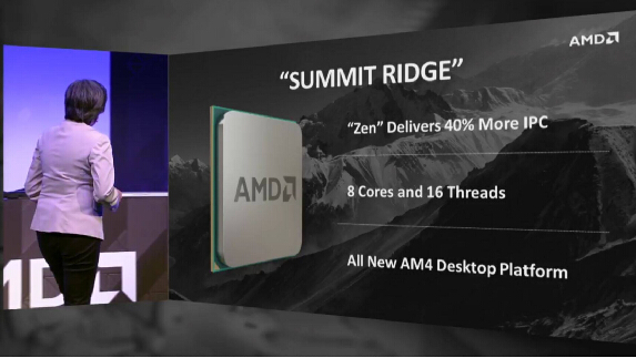
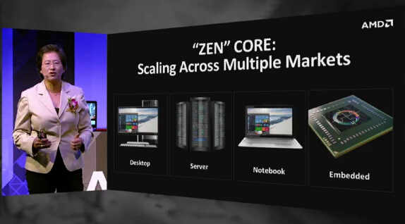
AMD debuted the world’s first live public demonstration of its revolutionary x86 “Zen” processor core architecture in the next-generation AM4 desktop processor (codenamed “Summit Ridge”) which features eight cores and sixteen threads. AMD’s “Zen” core is designed to scale across multiple markets including high-performance desktops, servers, notebooks and embedded solutions with first availability planned in our high-performance desktop “Summit Ridge” processor. via AMD【来自AMD的广告语,省略】
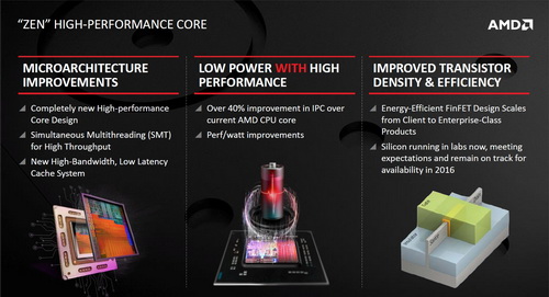
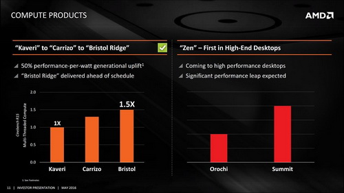
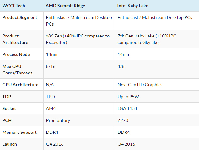
The AMD Summit Ridge FX-Series processor will house the new Zen architecture which is aiming to deliver up to 40% IPC (Instructions Per Clock) improvement over the existing Bulldozer architecture. AMD has confirmed that their Zen based Summit Ridge processors will feature 8 cores and 16 threads (SMT). The Summit Ridge chips are going to compete against Intel’s current generation products as AMD mentioned that they have achieved parity in performance against their age old competitor:
【新FX系列将采用Zen架构,在推土机架构基础上提供超过40%的IPC提升(实际上这几代CMT下来IPC提升也差不多这个数,这里应该说的是最新的Excavator。AMD已经确认Summit Ridge将会有8核心16线程(SMT)。AMD提到说,他们已经能和他们的老对手分庭抗礼:这意味着Summit Ridge将会与Intel目前的产品对抗。】
“By the end of the year, AMD will have moved on, to both its Zen CPU core as well as the Polaris graphics architecture. We are far closer to Intel than ever before ? you always need a number two to keep them honest,” said John Taylor. via ITWire
【“在今年年底前,AMD的CPU将会转移至Zen架构,同时显卡也会转移到Polaris架构。我们和Intel的距离,比以往任何时候都要近 – 你总需要一个千年老二来让他们保持老实(言外之意:而不是挤牙膏提价的JS“,John Taylor说。【AMD产品市场总监】
With Zen architecture, AMD plans to aim several different markets as its a scalable solution in design. AMD will first be shipping Zen in their Summit Ridge processors for enthusiast PCs. After that, AMD will be shipping Zen to server and workstations where we can see an even higher core count on Zen based Opteron processors. The AMD APU family will also get a taste of Zen on both desktops and mobility fronts next year.
【由于Zen架构设计上的可拓展性,AMD打算同时瞄准不同的市场。AMD将会首先为发烧友提供,在那之后是服务器和工作站,在这里我们可以看到更多核心的皓龙处理器。桌面和移动版APU也会在明年换上Zen架构。】
AMD Zen 14nm FinFET Process and Microarchitecture Details【Zen 14nm FinFET制程和微架构细节】
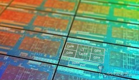
The Summit Ridge die is rectangular in shape. It houses two computing clusters placed at the opposite ends of the chip. Each computing cluster is comprised of four Zen cores. This rounds up to a total of eight Zen cores in each die. Each core in a given cluster of four shares L3 cache with the other three adjacent cores in the same cluster. In terms of other logic we can also see what appears to a DDR4 PHY placed in the lower left corner of the die. In addition to the DDR4 memory controller the Summit SOC also includes an integrated northbridge as well as numerous I/O logic.
【Summit Ridge的die是长方形的。在芯片两段放置着两个计算簇,每个计算簇都有四个Zen核心,加起来一共八个Zen核心。每个簇内四个核心共享同一块L3缓存。在其他逻辑方面,我们也能看到类似DDR4物理层的东西被放在芯片左下。在DDR4内存控制器之外,还有集成北桥以及一些I/O部分。】
Samsung’s 14nm FinFET process which Globalfoundries has licensed is going to be the basis of all of AMD’s next generation CPU, APU and GPU products. The company’s Chief Technology Officer Mark Papermaster made the announcement last year that the 14LPP process ? Samsung’s high performance 14nm process ? will be leveraged across all of AMD’s future products.
【GF从三星授权的14nm FinFET制程将会是AMD下代CPU,APU和GPU产品的基础。AMD的CTO Mark Papermaster去年就说,三星的高性能制程 – 14nmLPP 将会被应用在AMD未来的所有产品上。】
Mark Papermaster【PPTmaster】
FinFET technology is expected to play a critical foundational role across multiple AMD product lines, starting in 2016, GLOBALFOUNDRIES has worked tirelessly to reach this key milestone on its 14LPP process. We look forward to GLOBALFOUNDRIES’ continued progress towards full production readiness and expect to leverage the advanced 14LPP process technology across a broad set of our CPU, APU, and GPU products. ? Press Release
【FinFET技术将会在AMD多个产品线中扮演至关重要的角色。从2016年开始,GF就已经在尽全力达成14LPP制程这个关键性的里程碑。GF继续向着全面投产的方向前进,并且期望能在我们的CPU APU GPU上使用先进的14LPP制程。】
The 14LPP process features 3D finfet transistors and significantly smaller gates compared to 28nm. Chips manufactured on the 14LPP process have more than double the density of 28nm. Additionally, 14nm FinFET transistors are capable of significantly faster switching speeds. Products designed for the process will be able to achieve much higher frequencies than the same designs on 28nm. The process also delivers considerable power savings, essentially cutting power consumption by half. We can’t wait to hear more about Zen when it is close to launch.
【14LPP制程使用3D finfet晶体管,与28nm相比栅极大大缩小。14LPP制程的芯片,晶体管密度超过28nm两倍以上。此外,14nm FinFET晶体管的开关速度要快很多。用14LPP制程设计的芯片可以比用同样设计的28nm芯片达成更高的频率。14LPP也相当节能,基本上把功耗砍半。当Zen临近发布时,我们已经等不及想要听到关于它的更多消息了。】
来占位ZEN CPU的第一篇_(:3」 ∠)_